TMS320TCI6487
TMS320TCI6488
Communications Infrastructure Digital Signal Processor
www.ti.com
SPRS358F–APRIL 2007–REVISED AUGUST 2008
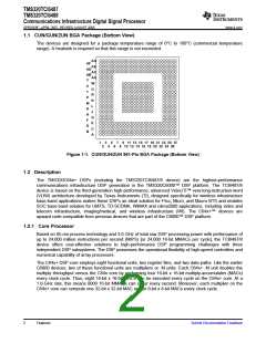
The TCI6487/8 DSP integrates a large amount of on-chip memory organized as a three-level memory
system. The level-1 data memories on the device are 32 KB each. This memory can be configured as
mapped RAM, cache, or some combination of the two. When configured as cache, L1 program (L1P) is a
direct-mapped cache where as L1 data (L1D) is a two-way set associative cache. The level-2 (L2)
memory is shared between program and data space for a total of 3 MB of SRAM/cache with two
configurations. L2 memory can be configured as 1 MB/1 MB/1 MB or 1.5 MB/1 MB/0.5 MB among the
three DSP cores. The level-3 (L3) ROM is 64 KB in the device. The C64x+ megamodule also has a 32-bit
peripheral configuration (CFG) port, an internal DMA (IDMA) controller, a system component with
reset/boot control, and a free-running 32-bit timer for time stamp.
The C64x+ DSP core has a complete set of development tools which includes: a new C compiler, an
assembly optimizer to simplify programming and scheduling, and a Windows® debugger interface for
visibility into source code execution.
The DMA switch fabric provides enhanced on-chip connectivity between the DSP cores and the
peripherals and accelerators.
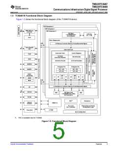
1.2.2 Peripherals
The peripheral set includes: an inter-integrated circuit bus module (I2C); two multichannel buffered serial
ports (McBSPs) each at 100 Mbps; six 64-bit general-purpose timers (also configurable as twelve 32-bit
timers); 16 general-purpose input/output ports (GPIO) with programmable interrupt/event generation
modes; an 1000 Ethernet media access controller (EMAC), which provides an efficient interface between
the TCI6487/8 DSP core processor and the network; a management data input/output (MDIO) module
(also part of EMAC), which is capable of interfacing to synchronous and asynchronous peripherals; a
frame synchronization (FSYNC) module, which synchronizes DMA transactions; a semaphore hardware
block (Semaphore), which allows access to shared resources with unique interrupts to each of the cores
to identify when that core has acquired the resource; and a 16-/32-bit DDR2 SDRAM interface.
The I2C port allows the DSP to easily control peripheral devices and communicate with a host processor.
The device includes two Serial RapidIO® (SRIO) with link rates of 1.25 Gbps, 2.5 Gbps or 3.125 Gbps.
This high bandwidth peripheral is used for point-to-point inter-device communication and may connect the
TCI6487/8 device to other DSPs, ASICs, or switches on the same board or across the backplane. This
dramatically improves system performance and reduces system cost for applications that include multiple
DSPs on a board such as video and telecom infrastructures and medical/imaging. The SRIO also provides
alarm, interrupt, and messaging events.
The device includes the SerDes-based antenna interface (AIF) capable of up to 3.072 Gbps operation per
link. The AIF comprises six high-speed serial links, compliant to OBSAI RP3 and CPRI standards. The
antenna interface is used to connect the backplane for antenna data transmission and reception. Each link
of the AIF includes a differential receive and transmit signal pair.
Submit Documentation Feedback
Features
3

 TI [ TEXAS INSTRUMENTS ]