TMS320TCI6487
TMS320TCI6488
Communications Infrastructure Digital Signal Processor
www.ti.com
SPRS358F–APRIL 2007–REVISED AUGUST 2008
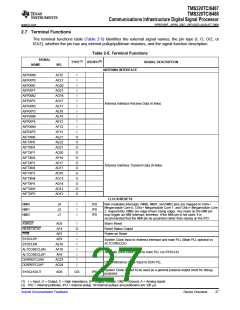
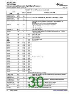
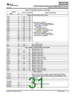
2.7 Terminal Functions
The terminal functions table (Table 2-5) identifies the external signal names, the pin type (I, O, O/Z, or
I/O/Z), whether the pin has any internal pullup/pulldown resistors, and the signal function description.
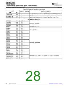
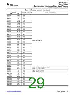
Table 2-5. Terminal Functions
SIGNAL
TYPE(1) IPD/IPU(2)
SIGNAL DESCRIPTION
NAME
NO.
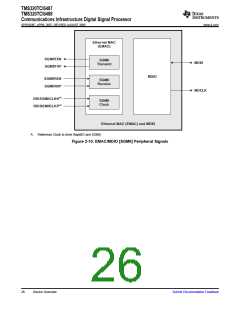
ANTENNA INTERFACE
AIFRXN0
AF22
AF21
AG20
AG21
AG18
AG17
AE17
AE18
AE14
AE13
AF12
AF13
AE21
AE22
AD21
AD20
AF16
AF17
AD17
AD16
AG13
AG14
AD13
AD12
I
I
AIFRXP0
AIFRXN1
AIFRXP1
AIFRXN2
AIFRXP2
AIFRXN3
AIFRXP3
AIFRXN4
AIFRXP4
AIFRXN5
AIFRXP5
AIFTXN0
AIFTXP0
AIFTXN1
AIFTXP1
AIFTXN2
AIFTXP2
AIFTXN3
AIFTXP3
AIFTXN4
AIFTXP4
AIFTXN5
AIFTXP5
I
I
I
I
Antenna Interface Receive Data (6 links)
I
I
I
I
I
I
O
O
O
O
O
O
O
O
O
O
O
O
Antenna Interface Transmit Data (6 links)
CLOCK/RESETS
NMI0
NMI1
NMI2
J4
J2
J1
I
I
I
IPD
IPD
IPD
Non-maskable interrupts. NMI0, NMI1, and NMI2 pins are mapped to C64x+
Megamodule Core 0, C64x+ Megamodule Core 1, and C64x+ Megamodule Core
2, respectively. NMIs are edge-driven (rising edge). Any noise on the NMI pin
may trigger an NMI interrupt; therefore, if the NMI pin is not used, it is
recommended that the NMI pin be grounded rather than relying on the IPD.
XWRST
AD5
AF4
I
O
I
Warm Reset
RESETSTAT
POR
Reset Status Output
Power-on Reset
AE5
SYSCLKP
AE9
I
System Clock Input to Antenna Interface and main PLL (Main PLL optional vs
ALTCORECLK)
SYSCLKN
AE10
AF10
AF9
I
ALTCORECLKN
ALTCORECLKP
DDRREFCLKN
DDRREFCLKP
I
Alternate Core Clock Input to main PLL (vs SYSCLK)
DDR Reference Clock Input to DDR PLL
I
AD23
AD24
I
I
System Clock Output to be used as a general purpose output clock for debug
purposes
SYSCLKOUT
AD6
O/Z
IPD
(1) I = Input, O = Output, Z = High impedance, S = Supply voltage, GND = Ground, A = Analog signal
(2) IPD = internal pulldown, IPU = internal pullup. All internal pullups and pulldowns are 100 µA.
Submit Documentation Feedback
Device Overview
27

 TI [ TEXAS INSTRUMENTS ]