TMS320TCI6487
TMS320TCI6488
Communications Infrastructure Digital Signal Processor
SPRS358F–APRIL 2007–REVISED AUGUST 2008
www.ti.com
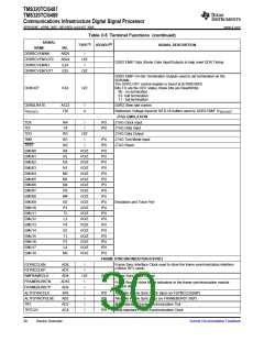
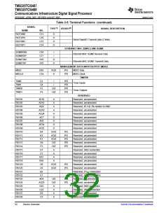
Table 2-5. Terminal Functions (continued)
SIGNAL
NAME
TYPE(1) IPD/IPU(2)
SIGNAL DESCRIPTION
NO.
AB25
AB24
E24
DDRRCVENIN0
DDRRCVENOUT0
DDRRCVENIN1
DDRRCVENOUT1
I
O/Z
I
DDR2 EMIF Data Strobe Gate Input/Outputs to help meet DDR Timing
E25
O/Z
DDR2 EMIF On-Die Termination Outputs used to set termination on the
SDRAMs
The DDR2 ODT control register is found at 0x7000 00F0
Bits 1:0 are the ODT status, these bits are Read/Write:
00 - no termination
DDRODT
K24
O/Z
01- half termination
11 - full termination
DDRSLRATE
VREFSSTL
AE23
T26
I
DDR2 Slew rate control
A
Reference Voltage Input for SSTL18 buffers used by DDR2 EMIF (VDDS18/2)
JTAG EMULATION
JTAG Clock Input
JTAG Data Input
JTAG Data Output
JTAG Test Mode Input
JTAG Reset
TCK
W4
V4
W3
W1
W2
R4
R2
N3
N1
M2
M1
N4
R3
M4
N2
R1
T2
I
IPU
IPU
TDI
I
TDO
O/Z
TMS
I
IPU
IPD
IPU
IPU
IPU
IPU
IPU
IPU
IPU
IPU
IPU
IPU
IPU
IPU
IPU
IPU
IPU
IPU
IPU
IPU
IPU
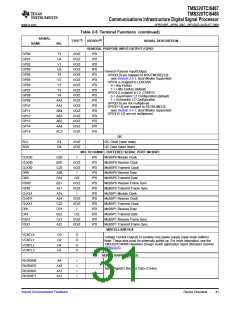
TRST
I
EMU00
EMU01
EMU02
EMU03
EMU04
EMU05
EMU06
EMU07
EMU08
EMU09
EMU10
EMU11
EMU12
EMU13
EMU14
EMU15
EMU16
EMU17
EMU18
I/O/Z
I/O/Z
I/O/Z
I/O/Z
I/O/Z
I/O/Z
I/O/Z
I/O/Z
I/O/Z
I/O/Z
I/O/Z
I/O/Z
I/O/Z
I/O/Z
I/O/Z
I/O/Z
I/O/Z
I/O/Z
I/O/Z
Emulation and Trace Port
L3
P4
K2
T1
P3
L4
M3
FRAME SYNCHRONIZATION (FSYNC)
FSYNCCLKN
FSYNCCLKP
SMFRAMECLK
FRAMEBURSTN
FRAMEBURSTP
ALTFSYNCCLK
ALTFSYNCPULSE
TRT
AD8
AD7
AD4
AD10
AD9
AF6
I
Frame Sync Interface Clock used to drive the frame synchronization interface
(OBSAI RP1 clock)
I
O/Z
IPD
Frame Sync Clock Output
I
I
I
I
I
I
Frame Burst to drive frame indicators to the frame synchronization module
(OBSAI RP1)
IPD
IPD
IPD
IPD
Alternate Frame Sync Clock Input (vs FSYNCCLK(N|P)
Alternate Frame Sync Input (vs FRAMEBURST (N|P)
Multi-standard Frame Synchronization Tick
AE6
AD3
AC4
TRTCLK
Multi-standard Frame Synchronization Clock
30
Device Overview
Submit Documentation Feedback

 TI [ TEXAS INSTRUMENTS ]