TMS320TCI6487
TMS320TCI6488
Communications Infrastructure Digital Signal Processor
SPRS358F–APRIL 2007–REVISED AUGUST 2008
www.ti.com
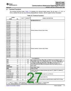
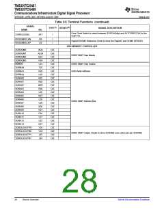
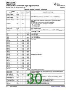
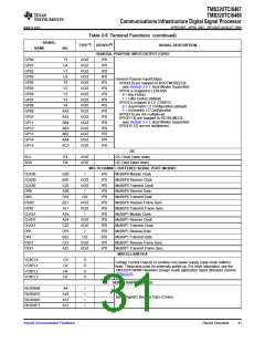
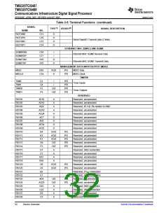
Table 2-5. Terminal Functions (continued)
SIGNAL
NAME
TYPE(1) IPD/IPU(2)
SIGNAL DESCRIPTION
NO.
Core Clock Select to select between SYSCLK(N|p) and ALTCORECCLK to the
main PLL
CORECLKSEL
AF7
I
RIOSGMIICLKN
RIOSGMIICLKP
D9
C9
I
I
RapidIO/SGMII Reference Clock to drive the RapidIO and SGMII SERDES
DDR MEMORY CONTROLLER
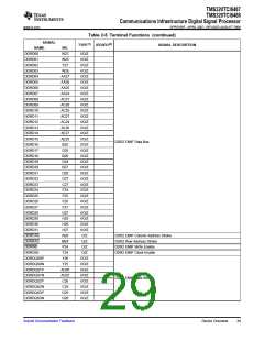
DDRDQM0
DDRDQM1
DDRDQM2
DDRDQM3
DDRCE
W24
AE24
B24
H24
L24
T25
R25
U25
K25
N25
M25
R26
L25
N27
L26
U26
K26
R27
P25
L27
U27
K27
V25
V24
J25
O/Z
O/Z
O/Z
O/Z
O/Z
O/Z
O/Z
O/Z
O/Z
O/Z
O/Z
O/Z
O/Z
O/Z
O/Z
O/Z
O/Z
O/Z
O/Z
O/Z
O/Z
O/Z
O/Z
O/Z
O/Z
O/Z
DDR2 EMIF Data Masks
DDR2 EMIF Chip Enable
DDR Bank Address
DDRBA0
DDRBA1
DDRBA2
DDRA00
DDRA01
DDRA02
DDRA03
DDRA04
DDRA05
DDRA06
DDR2 EMIF Address Bus
DDRA07
DDRA08
DDRA09
DDRA10
DDRA11
DDRA12
DDRA13
DDRCLKOUTP0
DDRCLKOUTN0
DDRCLKOUTP1
DDRCLKOUTN1
DDR2 EMIF Output Clocks to drive SDRAMs (one clock pair per SDRAM)
J24
28
Device Overview
Submit Documentation Feedback

 TI [ TEXAS INSTRUMENTS ]