TMS320TCI6487
TMS320TCI6488
Communications Infrastructure Digital Signal Processor
www.ti.com
SPRS358F–APRIL 2007–REVISED AUGUST 2008
8.19.3 IEEE 1149.1 JTAG
The JTAG interface is used to support boundary scan and emulation of the device. The boundary scan
supported allows for an asynchronous TRST and only the 5 baseline JTAG signals (e.g. no EMU[1:0])
required for boundary scan. Most interfaces on the device follow the Boundary Scan Test Specification
(IEEE1149.1), while all of the SerDes (Antenna Interface, RapidIO, and SGMII) support the AC coupled
net test defined in AC Coupled Net Test Specification (IEEE1149.6).
It is expected that all compliant devices are connected through the same JTAG interface, in daisy-chain
fashion, as per the specification. The JTAG interface uses 1.8-V buffers, compliant with the Power Supply
Voltage and Interface Standard for Nonterminated Digital Integrated Circuit Specification (EAI/JESD8-5).
8.19.3.1 IEEE 1149.1 JTAG Compatibility Statement
For maximum reliability, the TCI6487/8 DSP includes an internal pulldown (IPD) on the TRST pin to
ensure that TRST will always be asserted upon power up and the DSP's internal emulation logic will
always be properly initialized when this pin is not routed out. JTAG controllers from Texas Instruments
actively drive TRST high. However, some third-party JTAG controllers may not drive TRST high but expect
the use of an external pullup resistor on TRST. When using this type of JTAG controller, assert TRST to
initialize the DSP after powerup and externally drive TRST high before attempting any emulation or
boundary scan operations.
8.19.3.2 JTAG Electrical Data/Timing
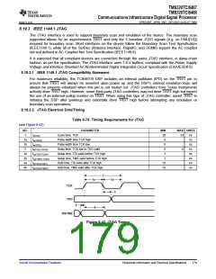
Table 8-74. Timing Requirements for JTAG
(see Figure 8-42)
NO.
1
PARAMETER
MIN
20
8
MAX UNITS
tc(TCK)
Cycle time, TCK
33
ns
ns
ns
ns
ns
ns
ns
ns
1a
1b
2
tw(TCKH)
Pulse width time TCK high
tw(TCKL)
Pulse width time TCK low
8
td(TCKL-TDOV)
tsu(TDIV-TCKH)
tsu(TMSV-TCKH)
th(TCKH-TDIV)
th(TCKH-TMSV)
Delay time, TCK low to TDO valid
Setup time, TDI valid before TCK high
Setup time, TMS valid before TCK high
Hold time, TDI valid after TCK high
Hold time, TMS valid after TCK high
0
8
3a
3b
4a
4b
2
2
10
10
1
1a
1b
TCK
TDO
2
3
4
TDI/TMS
Figure 8-42. JTAG Timing
Submit Documentation Feedback
Peripheral Information and Electrical Specifications
179

 TI [ TEXAS INSTRUMENTS ]