TMS320TCI6487
TMS320TCI6488
Communications Infrastructure Digital Signal Processor
www.ti.com
SPRS358F–APRIL 2007–REVISED AUGUST 2008
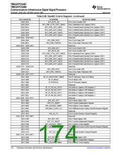
Table 8-68. RapidIO Control Registers (continued)
HEX ADDRESS
02D1 420C
02D1 4210
ACRONYM
REGISTER NAME
Port 2 Multicast-Event Control Symbol Request Register
Reserved
SP2_MULT_EVNT_CS
-
02D1 4214
SP2_CS_TX
Port 2 Control Symbol Transmit Register
Reserved
02D1 4218 - 02D1 42FC
02D1 4300
-
SP3_RST_OPT
Port 3 Reset Option CSR
02D1 4304
SP3_CTL_INDEP
Port 3 Control Independent Register
Port 3 Silence Timer Register
Port 3 Multicast-Event Control Symbol Request Register
Reserved
02D1 4308
SP3_SILENCE_TIMER
02D1 430C
SP3_MULT_EVNT_CS
02D1 4310
-
02D1 4314
SP3_CS_TX
Port 3 Control Symbol Transmit Register
Reserved
02D1 4318 - 02D2 0FFF
02D2 1000 - 02DF FFFF
-
-
Reserved
8.17.3 Serial RapidIO Electrical Data/Timing
Serial RapidIO is electrically compliant with the RapidIO™ Interconnect Specification, Part VI: Physical
Layer 1x/4x LP-Serial Specification, Revision 1.2.
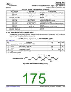
Table 8-69. Timing Requirements for SRIOSGMIIREFCLK(N|P)(1)
(see Figure 8-39)
NO.
PARAMETERS
MIN
MAX UNIT
1
tc(SRIOSGMIIREFCLK Cycle time, SRIOSGMIIREFCLK(N|P)
3.2
8
ns
)
2
3
4
5
tw(CLKH)
tw(CLKL)
tt(CLK)
Pulse duration, CLK(N|P) high
Pulse duration, CLK(N|P) low
Transition time, CLK(N|P)
0.4C
0.4C
50
ns
ns
ps
ps
1300
4
tj(CLK)
Period Jitter (RMS), CLK(N|P)
(1) C=1/SRIOSGMIIREFCLK(N|P)
1
4
2
SRIOSGMIIREFCLK(N|P)
3
4
Figure 8-39. SRIOSGMIIREFCLK(N|P) Timing
Submit Documentation Feedback
Peripheral Information and Electrical Specifications
175

 TI [ TEXAS INSTRUMENTS ]