TMS320TCI6487
TMS320TCI6488
Communications Infrastructure Digital Signal Processor
SPRS358F–APRIL 2007–REVISED AUGUST 2008
www.ti.com
8.18 General Purpose Input/Output (GPIO)
On the TCI6487/8 the GPIO peripheral pins GP[11:0] are used to latch configuration pins. These pins are
sampled at power-on reset and are functional as GPIO pins the remainder of the time. For more detailed
information on device/peripheral configuration and the TCI6487/8 device pin muxing, see Section 3,
Device Configuration.
8.18.1 GPIO Peripheral Register Description(s)
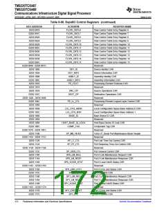
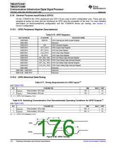
Table 8-70. GPIO Registers
HEX ADDRESS
02B0 0008
ACRONYM
BINTEN
-
REGISTER NAME
GPIO Interrupt per Bank Enable Register
02B0 000C
Reserved
02B0 0010
DIR
GPIO Direction Register
GPIO Output Data Register
GPIO Set Data Register
GPIO Clear Data Register
GPIO Input Data Register
02B0 0014
OUT_DATA
SET_DATA
CLR_DATA
IN_DATA
02B0 0018
02B0 001C
02B0 0020
02B0 0024
SET_RIS_TRIG GPIO Set Rising Edge Interrupt Register
CLR_RIS_TRIG GPIO Clear Rising Edge Interrupt Register
SET_FAL_TRIG GPIO Set Falling Edge Interrupt Register
CLR_FAL_TRIG GPIO Clear Falling Edge Interrupt Register
02B0 0028
02B0 002C
02B0 0030
02B0 008C
-
-
-
Reserved
Reserved
Reserved
02B0 0090 - 02B0 00FF
02B0 0100 - 02B0 3FFF
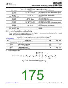
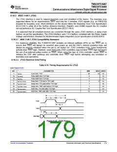
8.18.2 GPIO Electrical Data/Timing
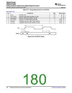
Table 8-71. Timing Requirements for GPIO Inputs(1)
(see Figure 8-40)
NO.
PARAMETER
MIN
12C - 3
12C - 3
MAX UNIT
1
2
tw(GPIH)
tw(GPIL)
Pulse duration, GPIx high
Pulse duration, GPIx low
ns
ns
(1) C = 1/CPU CLK frequency, in ns.
Table 8-72. Switching Characteristics Over Recommended Operating Conditions for GPIO Outputs(1)
(see Figure 8-40)
NO.
1
PARAMETER
Pulse duration, GPOx high
Pulse duration, GPOx low
MIN
36C - 8
36C - 8
MAX UNIT
tw(GPOH)
tw(GPOL)
ns
ns
2
(1) C = 1/CPU CLK frequency, in ns.
2
1
GPIx
4
3
GPOx
Figure 8-40. GPIO Timing
176
Peripheral Information and Electrical Specifications
Submit Documentation Feedback

 TI [ TEXAS INSTRUMENTS ]