TMS320F28027, TMS320F28027-Q1, TMS320F28027F, TMS320F28027F-Q1, TMS320F28026
TMS320F28026-Q1, TMS320F28026F, TMS320F28026F-Q1, TMS320F28023
TMS320F28023-Q1, TMS320F28022, TMS320F28021, TMS320F28020, TMS320F280200
ZHCSA13P –NOVEMBER 2008 –REVISED FEBRUARY 2021
www.ti.com.cn
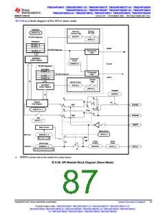
Enhanced feature:
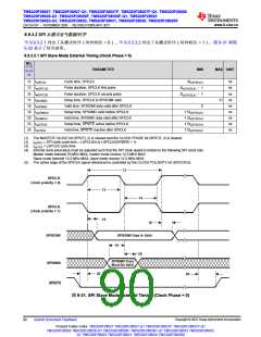
• 4-level transmit/receive FIFO
• Delayed transmit control
• Bidirectional 3 wire SPI mode support
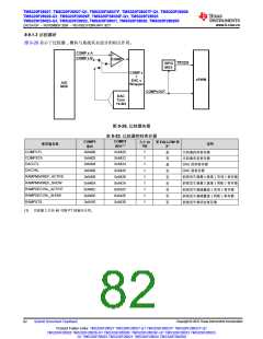
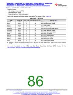
The SPI port operation is configured and controlled by the registers listed in 表9-24 .
表9-24. SPI-A Registers
NAME
SPICCR
ADDRESS
0x7040
0x7041
0x7042
0x7044
0x7046
0x7047
0x7048
0x7049
0x704A
0x704B
0x704C
0x704F
SIZE (x16) EALLOW PROTECTED
DESCRIPTION(1)
SPI-A Configuration Control Register
SPI-A Operation Control Register
SPI-A Status Register
1
1
1
1
1
1
1
1
1
1
1
1
No
No
No
No
No
No
No
No
No
No
No
No
SPICTL
SPISTS
SPIBRR
SPI-A Baud Rate Register
SPIRXEMU
SPIRXBUF
SPITXBUF
SPIDAT
SPI-A Receive Emulation Buffer Register
SPI-A Serial Input Buffer Register
SPI-A Serial Output Buffer Register
SPI-A Serial Data Register
SPIFFTX
SPIFFRX
SPIFFCT
SPIPRI
SPI-A FIFO Transmit Register
SPI-A FIFO Receive Register
SPI-A FIFO Control Register
SPI-A Priority Control Register
(1) Registers in this table are mapped to Peripheral Frame 2. This space only allows 16-bit accesses. 32-bit accesses produce undefined
results.
For more information on the SPI, see the Serial Peripheral Interface (SPI) chapter in the
TMS320F2802x,TMS320F2802xx Technical Reference Manual.
Copyright © 2022 Texas Instruments Incorporated
86
Submit Document Feedback
Product Folder Links: TMS320F28027 TMS320F28027-Q1 TMS320F28027F TMS320F28027F-Q1
TMS320F28026 TMS320F28026-Q1 TMS320F28026F TMS320F28026F-Q1 TMS320F28023 TMS320F28023-
Q1 TMS320F28022 TMS320F28021 TMS320F28020 TMS320F280200

 TI [ TEXAS INSTRUMENTS ]