TMS320F28027, TMS320F28027-Q1, TMS320F28027F, TMS320F28027F-Q1, TMS320F28026
TMS320F28026-Q1, TMS320F28026F, TMS320F28026F-Q1, TMS320F28023
TMS320F28023-Q1, TMS320F28022, TMS320F28021, TMS320F28020, TMS320F280200
ZHCSA13P –NOVEMBER 2008 –REVISED FEBRUARY 2021
www.ti.com.cn
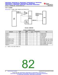
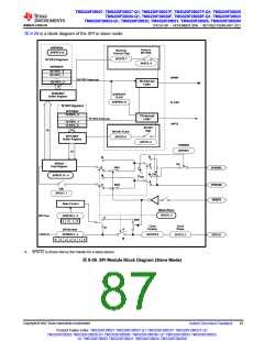
9.9.1.3.1 片载比较器/ DAC 电子数据/定时
9.9.1.3.1.1 Electrical Characteristics of the Comparator/DAC
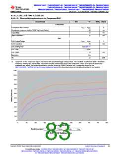
PARAMETER
MIN
TYP
MAX
UNITS
Comparator
Comparator Input Range
Comparator response time to PWM Trip Zone (Async)
Input Offset
V
V
V
SSA –VDDA
30
±5
35
ns
mV
mV
Input Hysteresis(1)
DAC
DAC Output Range
DAC resolution
DAC settling time
DAC Gain
V
SSA –VDDA
10
See 图9-27
–1.5%
10
bits
DAC Offset
Monotonic
mV
Yes
INL
±3
LSB
(1) Hysteresis on the comparator inputs is achieved with a Schmidt trigger configuration. This results in an effective 100-kΩfeedback
resistance between the output of the comparator and the noninverting input of the comparator. There is an option to disable the
hysteresis and, with it, the feedback resistance; see the Analog-to-Digital Converter and Comparator chapter in the
TMS320F2802x,TMS320F2802xx Technical Reference Manual for more information on this option if needed in your system.
1100
1000
900
800
700
600
500
400
300
200
100
0
0
50
100
150
200
250
300
350
400
450
500
DAC Step Size (Codes)
DAC Accuracy
15 Codes
7 Codes
3 Codes
1 Code
图9-27. DAC Settling Time
Copyright © 2022 Texas Instruments Incorporated
Submit Document Feedback
83
Product Folder Links: TMS320F28027 TMS320F28027-Q1 TMS320F28027F TMS320F28027F-Q1
TMS320F28026 TMS320F28026-Q1 TMS320F28026F TMS320F28026F-Q1 TMS320F28023 TMS320F28023-
Q1 TMS320F28022 TMS320F28021 TMS320F28020 TMS320F280200

 TI [ TEXAS INSTRUMENTS ]