TMS320F28027, TMS320F28027-Q1, TMS320F28027F, TMS320F28027F-Q1, TMS320F28026
TMS320F28026-Q1, TMS320F28026F, TMS320F28026F-Q1, TMS320F28023
TMS320F28023-Q1, TMS320F28022, TMS320F28021, TMS320F28020, TMS320F280200
ZHCSA13P –NOVEMBER 2008 –REVISED FEBRUARY 2021
www.ti.com.cn
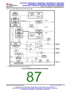
9.9.3 Serial Peripheral Interface (SPI) Module
The device includes the four-pin serial peripheral interface (SPI) module. One SPI module (SPI-A) is available.
The SPI is a high-speed, synchronous serial I/O port that allows a serial bit stream of programmed length (1 to
16 bits) to be shifted into and out of the device at a programmable bit-transfer rate. Normally, the SPI is used for
communications between the MCU and external peripherals or another processor. Typical applications include
external I/O or peripheral expansion through devices such as shift registers, display drivers, and ADCs.
Multidevice communications are supported by the master/slave operation of the SPI.
The SPI module features include:
• Four external pins:
– SPISOMI: SPI slave-output/master-input pin
– SPISIMO: SPI slave-input/master-output pin
– SPISTE: SPI slave transmit-enable pin
– SPICLK: SPI serial-clock pin
备注
All four pins can be used as GPIO if the SPI module is not used.
• Two operational modes: master and slave
Baud rate: 125 different programmable rates.
LSPCLK
Baud rate =
when SPIBRR = 3 to127
when SPIBRR = 0,1, 2
(SPIBRR + 1)
LSPCLK
4
Baud rate =
• Data word length: 1 to 16 data bits
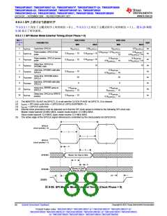
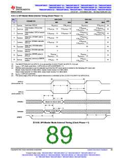
• Four clocking schemes (controlled by clock polarity and clock phase bits) include:
– Falling edge without phase delay: SPICLK active-high. SPI transmits data on the falling edge of the
SPICLK signal and receives data on the rising edge of the SPICLK signal.
– Falling edge with phase delay: SPICLK active-high. SPI transmits data one half-cycle ahead of the falling
edge of the SPICLK signal and receives data on the falling edge of the SPICLK signal.
– Rising edge without phase delay: SPICLK inactive-low. SPI transmits data on the rising edge of the
SPICLK signal and receives data on the falling edge of the SPICLK signal.
– Rising edge with phase delay: SPICLK inactive-low. SPI transmits data one half-cycle ahead of the rising
edge of the SPICLK signal and receives data on the rising edge of the SPICLK signal.
• Simultaneous receive and transmit operation (transmit function can be disabled in software)
• Transmitter and receiver operations are accomplished through either interrupt-driven or polled algorithms.
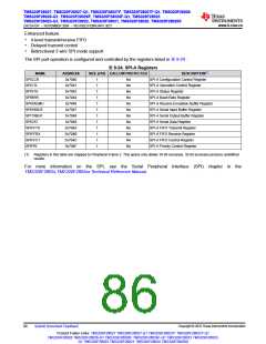
• Nine SPI module control registers: In control register frame beginning at address 7040h.
备注
All registers in this module are 16-bit registers that are connected to Peripheral Frame 2. When a
register is accessed, the register data is in the lower byte (7–0), and the upper byte (15–8) is
read as zeros. Writing to the upper byte has no effect.
Copyright © 2022 Texas Instruments Incorporated
Submit Document Feedback
85
Product Folder Links: TMS320F28027 TMS320F28027-Q1 TMS320F28027F TMS320F28027F-Q1
TMS320F28026 TMS320F28026-Q1 TMS320F28026F TMS320F28026F-Q1 TMS320F28023 TMS320F28023-
Q1 TMS320F28022 TMS320F28021 TMS320F28020 TMS320F280200

 TI [ TEXAS INSTRUMENTS ]