TMS320F28027, TMS320F28027-Q1, TMS320F28027F, TMS320F28027F-Q1, TMS320F28026
TMS320F28026-Q1, TMS320F28026F, TMS320F28026F-Q1, TMS320F28023
TMS320F28023-Q1, TMS320F28022, TMS320F28021, TMS320F28020, TMS320F280200
ZHCSA13P –NOVEMBER 2008 –REVISED FEBRUARY 2021
www.ti.com.cn
9.1.4 Real-Time JTAG and Analysis
1
The devices implement the standard IEEE 1149.1 JTAG interface for in-circuit based debug. Additionally, the
devices support real-time mode of operation allowing modification of the contents of memory, peripheral, and
register locations while the processor is running and executing code and servicing interrupts. The user can also
single step through non-time-critical code while enabling time-critical interrupts to be serviced without
interference. The device implements the real-time mode in hardware within the CPU. This is a feature unique to
the 28x family of devices, requiring no software monitor. Additionally, special analysis hardware is provided that
allows setting of hardware breakpoint or data/address watch-points and generating various user-selectable
break events when a match occurs. These devices do not support boundary scan; however, IDCODE and
BYPASS features are available if the following considerations are taken into account. The IDCODE does not
come by default. The user must go through a sequence of SHIFT IR and SHIFT DR state of JTAG to get the
IDCODE. For BYPASS instruction, the first shifted DR value would be 1.
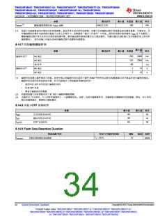
9.1.5 Flash
The F280200 device contains 8K × 16 of embedded flash memory, segregated into two 4K × 16 sectors. The
F28021/23/27 devices contain 32K × 16 of embedded flash memory, segregated into four 8K × 16 sectors. The
F28020/22/26 devices contain 16K × 16 of embedded flash memory, segregated into four 4K × 16 sectors. All
devices also contain a single 1K × 16 of OTP memory at address range 0x3D 7800 to 0x3D 7BFF. The user can
individually erase, program, and validate a flash sector while leaving other sectors untouched. However, it is not
possible to use one sector of the flash or the OTP to execute flash algorithms that erase/program other sectors.
Special memory pipelining is provided to enable the flash module to achieve higher performance. The flash/OTP
is mapped to both program and data space; therefore, it can be used to execute code or store data information.
Addresses 0x3F 7FF0 to 0x3F 7FF5 are reserved for data variables and should not contain program code.
备注
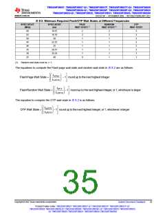
The Flash and OTP wait states can be configured by the application. This allows applications running
at slower frequencies to configure the flash to use fewer wait states.
Flash effective performance can be improved by enabling the flash pipeline mode in the Flash options
register. With this mode enabled, effective performance of linear code execution will be much faster
than the raw performance indicated by the wait-state configuration alone. The exact performance gain
when using the Flash pipeline mode is application-dependent.
For more information on the Flash options, Flash wait state, and OTP wait-state registers, see the
System Control chapter in the TMS320F2802x,TMS320F2802xx Technical Reference Manual.
9.1.6 M0,M1 SARAM
所有器件包含这两块单周期访问内存,每一个的大小为 1K x 16。复位时,堆栈指针指向块 M1 的开始位置。M0
和M1 块,与所有其它C28x 器件上的内存块一样,被映射到程序和数据空间。因此,用户能够使用M0 和M1 来
执行代码或者用于数据变量。分区在连接器内执行。C28x 器件提供了一个到编程器的统一内存映射。这使得用高
级语言编程变得更加容易。
9.1.7 L0 SARAM
此器件包含高达 4K x 16 的单周期访问 RAM。请参考节 9.2 中的器件专用内存映射图表来确定一个指定器件的准
确大小。这个块被映射到程序和数据空间。
1
IEEE Standard 1149.1-1990 Standard Test Access Port and Boundary Scan Architecture
Copyright © 2022 Texas Instruments Incorporated
Submit Document Feedback
37
Product Folder Links: TMS320F28027 TMS320F28027-Q1 TMS320F28027F TMS320F28027F-Q1
TMS320F28026 TMS320F28026-Q1 TMS320F28026F TMS320F28026F-Q1 TMS320F28023 TMS320F28023-
Q1 TMS320F28022 TMS320F28021 TMS320F28020 TMS320F280200

 TI [ TEXAS INSTRUMENTS ]