TMS320DM6437
Digital Media Processor
www.ti.com
SPRS345B–NOVEMBER 2006–REVISED MARCH 2007
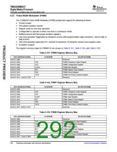
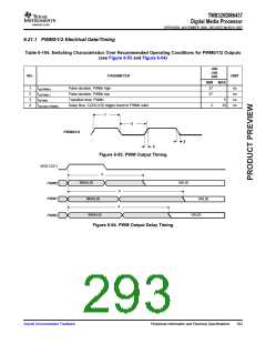
6.21.1 PWM0/1/2 Electrical Data/Timing
Table 6-104. Switching Characteristics Over Recommended Operating Conditions for PWM0/1/2 Outputs
(see Figure 6-53 and Figure 6-54)
-400
-500
-600
NO.
PARAMETER
UNIT
MIN
MAX
1
2
3
4
tw(PWMH)
tw(PWML)
Pulse duration, PWMx high
37
37
ns
ns
ns
ns
Pulse duration, PWMx low
tt(PWM)
Transition time, PWMx
5
td(CCDC-PWMV)
Delay time, CCDC(VD) trigger event to PWMx valid
2
10
1
2
PWM0/1/2
3
3
Figure 6-53. PWM Output Timing
VD(CCDC)
4
INVALID
VALID
PWM0
PWM1
4
INVALID
VALID
4
INVALID
VALID
PWM2
Figure 6-54. PWM Output Delay Timing
Submit Documentation Feedback
Peripheral Information and Electrical Specifications
293

 TI [ TEXAS INSTRUMENTS ]