TMS320DM6437
Digital Media Processor
www.ti.com
SPRS345B–NOVEMBER 2006–REVISED MARCH 2007
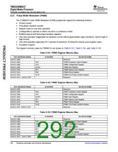
6.21 Pulse Width Modulator (PWM)
The 3 DM6437 Pulse Width Modulator (PWM) peripherals support the following features:
•
•
•
•
•
•
Period counter
First-phase duration counter
Repeat count for one-shot operation
Configurable to operate in either one-shot or continuous mode
Buffered period and first-phase duration registers
One-shot operation triggerable by hardware events with programmable edge transitions. (low-to-high or
high-to-low).
•
•
One-shot operation generates N+1 periods of waveform, N being the repeat count register value
Emulation support
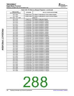
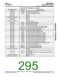
The register memory maps for PWM0/1/2 are shown in Table 6-101, Table 6-102, and Table 6-103.
Table 6-101. PWM0 Register Memory Map
HEX ADDRESS RANGE
0x01C2 2000
ACRONYM
REGISTER NAME
Reserved
0x01C2 2004
PCR
CFG
START
RPT
PER
PH1D
-
PWM0 Peripheral Control Register
PWM0 Configuration Register
PWM0 Start Register
0x01C2 2008
0x01C2 200C
0x01C2 2010
PWM0 Repeat Count Register
PWM0 Period Register
0x01C2 2014
0x01C2 2018
PWM0 First-Phase Duration Register
Reserved
0x01C2 201C - 0x01C2 23FF
Table 6-102. PWM1 Register Memory Map
HEX ADDRESS RANGE
0x01C2 2400
ACRONYM
REGISTER NAME
Reserved
0x01C2 2404
PCR
CFG
START
RPT
PER
PH1D
-
PWM1 Peripheral Control Register
0x01C2 2408
PWM1 Configuration Register
PWM1 Start Register
0x01C2 240C
0x01C2 2410
PWM1 Repeat Count Register
PWM1 Period Register
PWM1 First-Phase Duration Register
Reserved
0x01C2 2414
0x01C2 2418
0x01C2 241C -0x01C2 27FF
Table 6-103. PWM2 Register Memory Map
HEX ADDRESS RANGE
0x01C2 2800
ACRONYM
REGISTER NAME
Reserved
0x01C2 2804
PCR
CFG
START
RPT
PER
PH1D
-
PWM2 Peripheral Control Register
PWM2 Configuration Register
PWM2 Start Register
0x01C2 2808
0x01C2 280C
0x01C2 2810
PWM2 Repeat Count Register
PWM2 Period Register
0x01C2 2814
0x01C2 2818
PWM2 First-Phase Duration Register
Reserved
0x01C2 281C - 0x01C2 2BFF
292
Peripheral Information and Electrical Specifications
Submit Documentation Feedback

 TI [ TEXAS INSTRUMENTS ]