TMS320DM6437
Digital Media Processor
www.ti.com
SPRS345B–NOVEMBER 2006–REVISED MARCH 2007
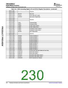
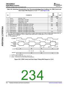
Table 6-45. Switching Characteristics Over Recommended Operating Conditions for VPBE Control and
Data Output With Respect to VCLK(1)(2)(3) (see Figure 6-26)
-400
-500
-600
NO.
PARAMETER
UNIT
MIN
MAX
17
18
19
20
21
22
23
24
25
26
tc(VCLK)
Cycle time, VCLK
13.33
0.4C
0.4C
160
ns
ns
ns
ns
ns
ns
ns
ns
ns
ns
tw(VCLKH)
Pulse duration, VCLK high
tw(VCLKL)
Pulse duration, VCLK low
tt(VCLK)
Transition time, VCLK
TBD
TBD
TBD
7
td(VCLKINH-VCLKH)
td(VCLKINL-VCLKL)
td(VCLK-VCTLV)
td(VCLK-VCTLIV)
td(VCLK-VDATAV)
td(VCLK-VDATAIV)
Delay time, VCLKIN high to VCLK high
Delay time, VCLKIN low to VCLK low
Delay time, VCLK edge to VCTL valid
Delay time, VCLK edge to VCTL invalid
Delay time, VCLK edge to VDATA valid
Delay time, VCLK edge to VDATA invalid
TBD
TBD
0.6
0.6
7
(1) The VPBE may be configured to operate in either positive or negative edge clocking mode. When in positive edge clocking mode, the
rising edge of VCLK is referenced. When in negative edge clocking mode, the falling edge of VCLK is referenced.
(2) VCLKIN = PCLK or VPBECLK
(3) C = VCLK period in ns.
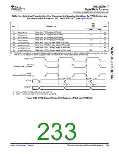
(A)
VCLKIN
18
21
17
22
19
VCLK
(Positive Edge
Clocking)
VCLK
(Negative Edge
Clocking)
20
23
25
20
24
26
(B)
VCTL
(C)
VDATA
A. VCLKIN = PCLK or VPBECLK
B. VCTL = HSYNC, VSYNC, LCD_FIELD, and LCD_OE
C. VDATA = COUT[7:0], YOUT[7:0], R[7:0], G[7:0], and B[7:0]
Figure 6-26. VPBE Control and Data Output Timing With Respect to VCLK
234
Peripheral Information and Electrical Specifications
Submit Documentation Feedback

 TI [ TEXAS INSTRUMENTS ]