TMS320DM6437
Digital Media Processor
www.ti.com
SPRS345B–NOVEMBER 2006–REVISED MARCH 2007
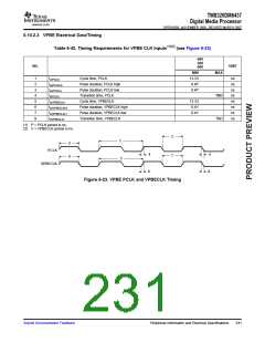
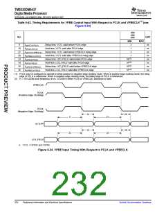
Table 6-43. Timing Requirements for VPBE Control Input With Respect to PCLK and VPBECLK(1) (see
Figure 6-24)
-400
-500
-600
NO.
UNIT
MIN
MAX
9
tsu(VCTLV-PCLK)
th(PCLK-VCTLV)
Setup time, VCTL valid before PCLK edge
3
1
ns
ns
ns
ns
ns
ns
ns
ns
10
27
28
33
34
35
36
Hold time, VCTL valid after PCLK edge
tsu(VCTLV-VPBECLK)
th(VPBECLK-VCTLV)
tsu(FIELD-PCLK)
Setup time, VCTL valid before VPBECLK rising edge
Hold time, VCTL valid after VPBECLK rising edge
Setup time, LCD_FIELD valid before PCLK edge
Hold time, LCD_FIELD valid after PCLK edge
Setup time, LCD_FIELD valid before VPBECLK edge
Hold time, LCD_FIELD valid after VPBECLK edge
3
1
5P(2)
5P(2)
5P(2)
5P(2)
th(PCLK-FIELD)
tsu(FIELD-VPBECLK)
th(VPBECLK-FIELD)
(1) PCLK may be configured to operate in either positive or negative edge clocking mode. When in positive edge clocking mode, the rising
edge of PCLK is referenced. When in negative edge clocking mode, the falling edge of PCLK is referenced.
(2) P = 1/(VCLKIN clock frequency) in ns. VCLKIN is either PCLK or VPBECLK, whichever is used.
VPBECLK
PCLK
(Positive Edge Clocking)
PCLK
(Negative Edge Clocking)
10
34
28
36
9
27
35
(A)
VCTL
33
LCD_FIELD
A. VCTL = HSYNC and VSYNC
Figure 6-24. VPBE Input Timing With Respect to PCLK and VPBECLK
232
Peripheral Information and Electrical Specifications
Submit Documentation Feedback

 TI [ TEXAS INSTRUMENTS ]