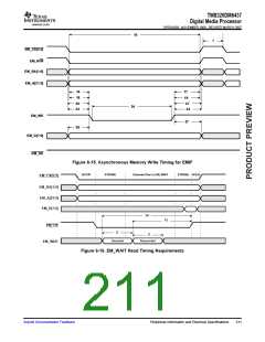
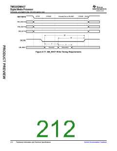
TMS320DM6437
Digital Media Processor
www.ti.com
SPRS345B–NOVEMBER 2006–REVISED MARCH 2007
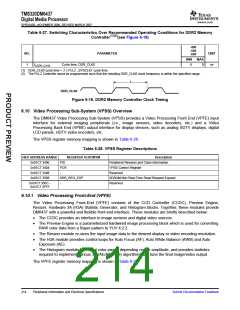
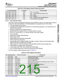
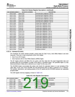
Table 6-29. VPFE Register Address Range Descriptions
HEX ADDRESS RANGE
0x01C7 0400 – 0x01C7 07FF
0x01C7 0800 – 0x01C7 0BFF
0x01C7 0C00 – 0x01C7 09FF
0x01C7 1000 – 0x01C7 13FF
0x01C7 1400 – 0x01C7 17FF
0x01C7 3400 – 0x01C7 3FFF
ACRONYM
CCDC
PREV
RESZ
HIST
REGISTER NAME
VPFE – CCD Controller
VPFE – Preview Engine/Image Signal Processor
VPFE – Resizer
VPFE – Histogram
H3A
VPFE – Hardware 3A (Auto-Focus/WB/Exposure)
VPSS Shared Buffer Logic Registers
VPSS
6.10.1.1 CCD Controller (CCDC)
The CCDC receives raw image/video data from sensors (CMOS or CCD) or YUV video data in numerous
formats from video decoder devices. The following features are supported by the CCDC module.
•
•
Conventional Bayer pattern format.
Generates HD/VD timing signals and field ID to an external timing generator or can synchronize to an
external timing generator.
•
•
•
•
•
•
•
•
•
Interface to progressive and interlaced sensors.
REC656/CCIR-656 standard (YCbCr 4:2:2 format, either 8- or 16-bit).
YCbCr 4:2:2 format, either 8- or 16-bit with discrete H and VSYNC signals.
Up to 16-bit input.
Optical black clamping signal generation.
Shutter signal control.
Digital clamping and black level compensation.
10-bit to 8-bit A-law compression.
Low-pass filter prior to writing to SDRAM. If this filter is enabled, 2 pixels each in the left and right
edges of each line are cropped from the output.
•
•
•
•
Output range from 16-bits to 8-bits wide (8-bits wide allows for 50% saving in storage area).
Downsampling via programmable culling patterns.
Control output to the DDR2 via an external write enable signal.
Up to 16K pixels (image size) in both the horizontal and vertical direction.
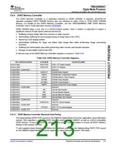
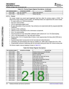
The CCDC register memory mapping is shown in Table 6-30.
Table 6-30. CCDC Register Descriptions
HEX ADDRESS RANGE
REGISTER ACRONYM
DESCRIPTION
0x01C7 0400
0x01C7 0404
0x01C7 0408
0x01C7 040C
0x01C7 0410
0x01C7 0414
0x01C7 0418
0x01C7 041C
0x01C7 0420
0x01C7 0424
0x01C7 0428
0x01C7 042C
0x01C7 0430
0x01C7 0434
PID
Peripheral Revision and Class Information
Peripheral Control Register
PCR
SYN_MODE
HD_VD_WID
PIX_LINES
HORZ_INFO
VERT_START
VERT_LINES
CULLING
SYNC and Mode Set Register
HD and VD Signal Width
Number of Pixels in a Horizontal Line and Number of Lines in a Frame
Horizontal Pixel Information
Vertical Line - Settings for the Starting Pixel
Number of Vertical Lines
Culling Information in Horizontal and Vertical Directions
Horizontal Size
HSIZE_OFF
SDOFST
SDRAM/DDRAM Line Offset
SDR_ADDR
CLAMP
SDRAM Address
Optical Black Clamping Settings
DC Clamp
DCSUB
Submit Documentation Feedback
Peripheral Information and Electrical Specifications
215

 TI [ TEXAS INSTRUMENTS ]