TMS320DM6437
Digital Media Processor
www.ti.com
SPRS345B–NOVEMBER 2006–REVISED MARCH 2007
6.9.4 DDR2 Memory Controller
The DDR2 Memory Controller is a dedicated interface to DDR2 SDRAM. It supports JESD79D-2A
standard compliant DDR2 SDRAM Devices and can interface to either 16-bit or 32-bit DDR2 SDRAM
devices. For details on the DDR2 Memory Controller, see the TMS320DM643x DMP DDR2 Memory
Controller User’s Guide (literature number SPRU986).
DDR2 SDRAM plays a key role in a DaVinci-based system. Such a system is expected to require a
significant amount of high-speed external memory for:
•
•
•
•
Buffering of input image data from sensors or video sources
Intermediate buffering for processing/resizing of image data in the VPFE
Numerous OSD display buffers
Intermediate buffering for large raw Bayer data image files while performing image processing
functions
•
•
Buffering for intermediate data while performing video encode and decode functions
Storage of executable code for the DSP
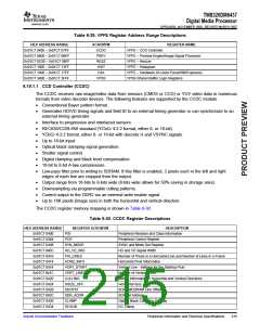
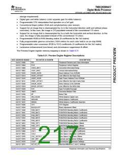
A memory map of the DDR2 Memory Controller registers is shown in Table 6-26.
Table 6-26. DDR2 Memory Controller Registers
HEX ADDRESS RANGE
0x01C4 004C
ACRONYM
DDRVTPER
DDRVTPR
-
REGISTER NAME
DDR2 VTP Enable Register
DDR2 VTP Register
Reserved
0x01C4 2038
0x2000 0000 - 0x2000 0003
0x2000 0004
SDRSTAT
SDBCR
SDRCR
SDTIMR
SDTIMR2
PBBPR
-
SDRAM Status Register
0x2000 0008
SDRAM Bank Configuration Register
SDRAM Refresh Control Register
SDRAM Timing Register
SDRAM Timing Register 2
Peripheral Bus Burst Priority Register
Reserved
0x2000 000C
0x2000 0010
0x2000 0014
0x2000 0020
0x2000 0024 - 0x2000 00BF
0x2000 00C0
IRR
Interrupt Raw Register
Interrupt Masked Register
Interrupt Mask Set Register
Interrupt Mask Clear Register
Reserved
0x2000 00C4
IMR
0x2000 00C8
IMSR
0x2000 00CC
IMCR
0x2000 00D0 - 0x2000 00E3
0x2000 00E4
-
DDRPHYCR
-
DDR PHY Control Register
Reserved
0x2000 00E8 - 0x2000 00EF
0x2000 00F0
VTPIOCR
-
DDR VTP IO Control Register
Reserved
0x2000 00F4 - 0x2000 7FFF
6.9.4.1 DDR2 Memory Controller Electrical Data/Timing
The Implementing DDR2 PCB Layout on the DM643x Digital Media Processor application report (literature
number TBD) specifies a complete DDR2 interface solution for the DM6437 as well as a list of compatible
DDR2 devices. TI has performed the simulation and system characterization to ensure all DDR2 interface
timings in this solution are met.
TI only supports board designs that follow the guidelines outlined in the Implementing DDR2 PCB Layout
on the DM643x Digital Media Processor application report (literature number TBD ulink).
Submit Documentation Feedback
Peripheral Information and Electrical Specifications
213

 TI [ TEXAS INSTRUMENTS ]