TMS320C6678
Multicore Fixed and Floating-Point Digital Signal Processor
SPRS691D—April 2013
www.ti.com
7.27.3 IEEE 1149.1 JTAG
The JTAG interface is used to support boundary scan and emulation of the device. The boundary scan supported
allows for an asynchronous TRST and only the 5 baseline JTAG signals (e.g., no EMU[1:0]) required for boundary
scan. Most interfaces on the device follow the Boundary Scan Test Specification (IEEE1149.1), while all of the SerDes
(SRIO and SGMII) support the AC-coupled net test defined in AC-Coupled Net Test Specification (IEEE1149.6).
It is expected that all compliant devices are connected through the same JTAG interface, in daisy-chain fashion, in
accordance with the specification. The JTAG interface uses 1.8-V LVCMOS buffers, compliant with the Power
Supply Voltage and Interface Standard for Nonterminated Digital Integrated Circuit Specification (EAI/JESD8-5).
7.27.3.1 IEEE 1149.1 JTAG Compatibility Statement
For maximum reliability, the C6678 DSP includes an internal pulldown (IPD) on the TRST pin to ensure that TRST
will always be asserted upon power up and the DSP's internal emulation logic will always be properly initialized
when this pin is not routed out. JTAG controllers from Texas Instruments actively drive TRST high. However, some
third-party JTAG controllers may not drive TRST high but expect the use of an external pullup resistor on TRST.
When using this type of JTAG controller, assert TRST to initialize the DSP after powerup and externally drive TRST
high before attempting any emulation or boundary scan operations.
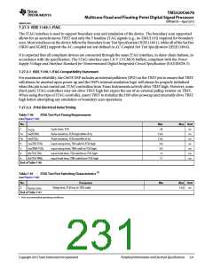
7.27.3.2 JTAG Electrical Data/Timing
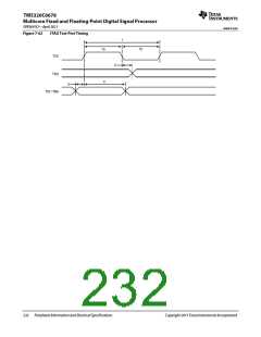
Table 7-90
(see Figure 7-62)
JTAG Test Port Timing Requirements
No.
Min
34
Max Unit
1
tc(TCK)
Cycle time, TCK
ns
ns
ns
ns
ns
ns
ns
1a
1b
3
tw(TCKH)
tw(TCKL)
Pulse duration, TCK high (40% of tc)
Pulse duration, TCK low(40% of tc)
13.6
13.6
3.4
3.4
17
tsu(TDI-TCK)
tsu(TMS-TCK)
th(TCK-TDI)
th(TCK-TMS)
input setup time, TDI valid to TCK high
input setup time, TMS valid to TCK high
input hold time, TDI valid from TCK high
input hold time, TMS valid from TCK high
3
4
4
17
End of Table 7-90
Table 7-91
JTAG Test Port Switching Characteristics (1)
Parameter
(see Figure 7-62)
No.
Min
Max Unit
2
td(TCKL-TDOV)
Delay time, TCK low to TDO valid
13.6
ns
End of Table 7-91
1 Over recommended operating conditions.
Copyright 2013 Texas Instruments Incorporated
Peripheral Information and Electrical Specifications 231

 TI [ TEXAS INSTRUMENTS ]