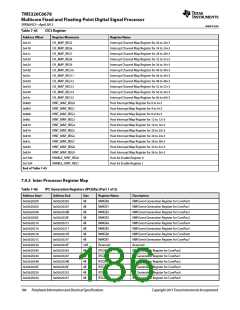
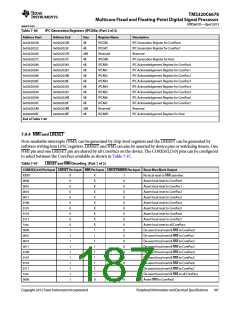
TMS320C6678
Multicore Fixed and Floating-Point Digital Signal Processor
SPRS691D—April 2013
www.ti.com
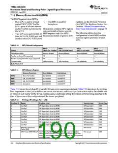
7.10 Memory Protection Unit (MPU)
The C6678 supports four MPUs:
•
•
One MPU is used to protect
main CORE/3 CFG TeraNet
(CFG space of all slave devices
•
One MPU is used for
Semaphore.
registers, see the Memory Protection
Unit (MPU) for KeyStone Devices User
Guide in ‘‘Related Documentation
on the TeraNet is protected by This section contains MPU register from Texas Instruments’’ on page 73.
the MPU).
map and details of device-specific
MPU registers only. For MPU
The following tables show the
configuration of each MPU and the
memory regions protected by each
MPU.
Two MPUs are used for QM_SS
(one for DATA PORT port and
another is for CFG PORT port).
features and details of generic MPU
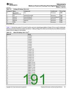
Table 7-50
Setting
MPU Default Configuration
MPU0
MPU1
MPU2
(QM_SS CFG PORT)
MPU3
(Semaphore)
(Main CFG TeraNet) (QM_SS DATA PORT)
Default permission
Assume allowed
Assume allowed
Assume allowed
Assume allowed
Number of allowed IDs supported
Number of programmable ranges supported
Compare width
16
16
16
16
16
5
16
1
1KB granularity
1KB granularity
1KB granularity
1KB granularity
End of Table 7-50
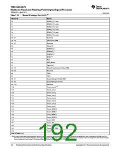
Table 7-51
MPU Memory Regions
Memory Protection
Main CFG TeraNet
QM_SS DATA PORT
QM_SS CFG PORT
Semaphore
Start Address
0x01D00000
0x34000000
0x02A00000
0x02640000
End Address
0x026207FF
0x340BFFFF
0x02ABFFFF
0x026407FF
MPU0
MPU1
MPU2
MPU3
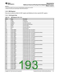
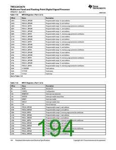
Table 7-52 shows the privilege ID of each CORE and every mastering peripheral. Table 7-52 also shows the privilege
level (supervisor vs. user), security level (secure vs. non-secure), and access type (instruction read vs. data/DMA read
or write) of each master on the device. In some cases, a particular setting depends on software being executed at the
time of the access or the configuration of the master peripheral.
Table 7-52
Privilege ID Settings (Part 1 of 2)
Privilege ID Master
Privilege Level
Security Level
SW dependant
SW dependant
SW dependant
SW dependant
SW dependant
SW dependant
SW dependant
SW dependant
Non-secure
Access Type
DMA
0
1
2
3
4
5
6
7
8
CorePac0
CorePac1
CorePac2
CorePac3
CorePac4
CorePac5
CorePac6
CorePac7
SW dependant, driven by MSMC
SW dependant, driven by MSMC
SW dependant, driven by MSMC
SW dependant, driven by MSMC
SW dependant, driven by MSMC
SW dependant, driven by MSMC
SW dependant, driven by MSMC
SW dependant, driven by MSMC
User
DMA
DMA
DMA
DMA
DMA
DMA
DMA
Network Coprocessor
Packet DMA
DMA
9
SRIO Packet DMA/SRIO_M User/Driven by SRIO block, User mode and supervisor mode is
determined on a per-transaction basis. Only the transaction with
source ID matching the value in the SupervisorID register is granted
supervisor mode.
Non-secure
DMA
190
Peripheral Information and Electrical Specifications
Copyright 2013 Texas Instruments Incorporated

 TI [ TEXAS INSTRUMENTS ]