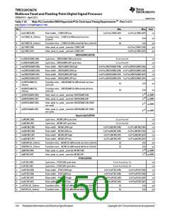
TMS320C6678
Multicore Fixed and Floating-Point Digital Signal Processor
SPRS691D—April 2013
www.ti.com
7.7 PASS PLL
The PASS PLL generates interface clocks for the Network Coprocessor. Using the PACLKSEL pin the user can select
the input source of PASS PLL as either the output of CORECLK clock reference sources or the PASSCLK clock
reference sources. When coming out of power-on reset, PASS PLL comes out in a bypass mode and needs to be
programmed to a valid frequency before being enabled and used.
PASS PLL power is supplied via the PASS PLL power-supply pin (AVDDA3). An external EMI filter circuit must be
added to all PLL supplies. Please see the Hardware Design Guide for KeyStone Devices in ‘‘Related Documentation
from Texas Instruments’’ on page 73. for detailed recommendations. For the best performance, TI recommends that
all the PLL external components be on a single side of the board without jumpers, switches, or components other
than those shown. For reduced PLL jitter, maximize the spacing between switching signal traces and the PLL
external components (C1, C2, and the EMI Filter).
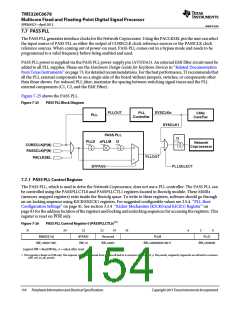
Figure 7-25 shows the PASS PLL.
Figure 7-25
PASS PLL Block Diagram
PLLOUT
SYSCLKn
PLL
Controller
C66x
CorePac
PLL
SYSCLK1
PASS PLL
/3
PLLD xPLLM /2
Network
Coprocessor
CORECLK(P|N)
0
PASSCLK(P|N)
PACLKSEL
PLLOUT
1
BYPASS
PLLSELECT
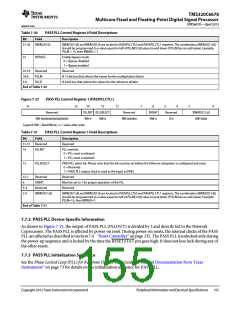
7.7.1 PASS PLL Control Register
The PASS PLL, which is used to drive the Network Coprocessor, does not use a PLL controller. The PASS PLL can
be controlled using the PASSPLLCTL0 and PASSPLLCTL1 registers located in Bootcfg module. These MMRs
(memory-mapped registers) exist inside the Bootcfg space. To write to these registers, software should go through
an un-locking sequence using KICK0/KICK1 registers. For suggested configurable values see 2.5.4 ‘‘PLL Boot
Configuration Settings’’ on page 41. See section 3.3.4 ‘‘Kicker Mechanism (KICK0 and KICK1) Register’’ on
page 81 for the address location of the registers and locking and unlocking sequences for accessing the registers. This
register is reset on POR only.
.
Figure 7-26
PASS PLL Control Register 0 (PASSPLLCTL0) (1)
31
24
23
22
Reserved
RW,+0001
19
18
6
5
0
BWADJ[7:0]
RW,+0000 1001
BYPASS
RW,+0
PLLM
PLLD
RW,+000000
RW,+0000000010011
Legend: RW = Read/Write; -n = value after reset
1 This register is Reset on POR only. The regreset, reset and bgreset from PLL are all tied to a common pll0_ctrl_rst_n The pwrdn, regpwrdn, bgpwrdn are all tied to common
pll0_ctrl_to_pll_pwrdn.
154
Peripheral Information and Electrical Specifications
Copyright 2013 Texas Instruments Incorporated

 TI [ TEXAS INSTRUMENTS ]