TMS320C6678
Multicore Fixed and Floating-Point Digital Signal Processor
SPRS691D—April 2013
www.ti.com
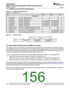
7.8.2 EDMA3 Channel Controller Configuration
Table 7-33 provides the configuration for each of the EDMA3 channel controllers present on the device.
Table 7-33
Description
EDMA3 Channel Controller Configuration
EDMA3 CC0 EDMA3 CC1 EDMA3 CC2
Number of DMA channels in Channel Controller
Number of QDMA channels
16
8
64
8
64
8
Number of interrupt channels
Number of PaRAM set entries
16
128
2
64
512
4
64
512
4
Number of event queues
Number of Transfer Controllers
Memory Protection Existence
Number of Memory Protection and Shadow Regions
End of Table 7-33
2
4
4
Yes
8
Yes
8
Yes
8
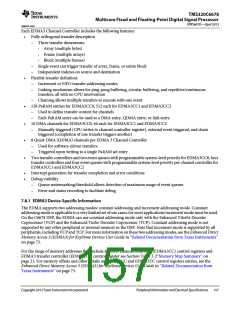
7.8.3 EDMA3 Transfer Controller Configuration
Each transfer controller on a device is designed differently based on considerations like performance requirements,
system topology (like main TeraNet bus width, external memory bus width), etc. The parameters that determine the
transfer controller configurations are:
•
FIFOSIZE: Determines the size in bytes for the data FIFO that is the temporary buffer for the in-flight data.
The data FIFO is where the read return data read by the TC read controller from the source endpoint is stored
and subsequently written out to the destination endpoint by the TC write controller.
•
•
•
BUSWIDTH: The width of the read and write data buses in bytes, for the TC read and write controller,
respectively. This is typically equal to the bus width of the main TeraNet interface.
Default Burst Size (DBS): The DBS is the maximum number of bytes per read/write command issued by a
transfer controller.
DSTREGDEPTH: This determines the number of destination FIFO register set. The number of destination
FIFO register set for a transfer controller determines the maximum number of outstanding transfer requests.
All four parameters listed above are fixed by the design of the device.
Table 7-34 provides the configuration for each of the EDMA3 transfer controllers present on the device.
Table 7-34
EDMA3 Transfer Controller Configuration
EDMA3 CC0
TC1
EDMA3 CC1
TC2
EDMA3 CC2
TC2
Parameter
FIFOSIZE
TC0
TC0
TC1
TC3
TC0
TC1
TC3
1024 bytes 1024 bytes 1024 bytes 512 bytes 1024 bytes 512 bytes 1024 bytes 512 bytes 512 bytes 1024 bytes
BUSWIDTH
32 bytes
32 bytes
4 entries
128 bytes
16 bytes
4 entries
128 bytes
16 bytes
4 entries
64 bytes
16 bytes
4 entries
128 bytes
16 bytes
4 entries
64 bytes
16 bytes
4 entries
128 bytes
16 bytes
4 entries
64 bytes
16 bytes
4 entries
64 bytes
16 bytes
4 entries
128 bytes
DSTREGDEPTH 4 entries
DBS 128 bytes
End of Table 7-34
7.8.4 EDMA3 Channel Synchronization Events
The EDMA3 supports up to 16 DMA channels for EDMA3CC0, 64 each for EDMA3CC1 and EDMA3CC2 that can
be used to service system peripherals and to move data between system memories. DMA channels can be triggered
by synchronization events generated by system peripherals. The following tables lists the source of the
synchronization event associated with each of the EDMA EDMA3CC DMA channels. On the C6678, the association
of each synchronization event and DMA channel is fixed and cannot be reprogrammed.
158
Peripheral Information and Electrical Specifications
Copyright 2013 Texas Instruments Incorporated

 TI [ TEXAS INSTRUMENTS ]