TMS320C6678
Multicore Fixed and Floating-Point Digital Signal Processor
SPRS691D—April 2013
www.ti.com
7.6.2 DDR3 PLL Device-Specific Information
As shown in Figure 7-21, the output of DDR3 PLL (PLLOUT) is divided by 2 and directly fed to the DDR3 memory
controller. The DDR3 PLL is affected by power-on reset. During power-on resets, the internal clocks of the DDR3
PLL are affected as described in Section 7.4 ‘‘Reset Controller’’ on page 132. DDR3 PLL is unlocked only during the
power-up sequence and is locked by the time the RESETSTAT pin goes high. It does not lose lock during any of the
other resets.
7.6.3 DDR3 PLL Initialization Sequence
See the Phase Locked Loop (PLL) for KeyStone Devices User Guide in ‘‘Related Documentation from Texas
Instruments’’ on page 73 for details on the initialization sequence for DDR3 PLL.
Note—DDR3 interface needs to reset every time the DDR3 PLL is re-programmed.
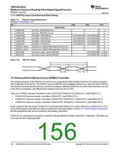
7.6.4 DDR3 PLL Input Clock Electrical Data/Timing
Table 7-29
DDR3 PLL DDRSYSCLK1(N|P) Timing Requirements
(see Figure 7-24 and Figure 7-20)
No.
Min
Max Unit
DDRCLK[P:N]
1
1
3
2
2
3
4
4
5
5
tc(DDRCLKN)
tc(DDRCLKP)
Cycle time _ DDRCLKN cycle time
Cycle time _ DDRCLKP cycle time
Pulse width _ DDRCLKN high
Pulse width _ DDRCLKN low
Pulse width _ DDRCLKP high
Pulse width _ DDRCLKP low
3.2
3.2
25
25
ns
ns
ns
ns
ns
ns
ps
ps
ps
ps
tw(DDRCLKN)
tw(DDRCLKN)
tw(DDRCLKP)
tw(DDRCLKP)
tr(DDRCLK_250mv)
tf(DDRCLK_250mv)
tj(DDRCLKN)
0.45*tc(DDRCLKN)
0.45*tc(DDRCLKN)
0.45*tc(DDRCLKP)
0.45*tc(DDRCLKP)
50
0.55*tc(DDRCLKN)
0.55*tc(DDRCLKN)
0.55*tc(DDRCLKP)
0.55*tc(DDRCLKP)
350
Transition time _ DDRCLK differential rise time (250 mV)
Transition time _ DDRCLK differential fall time (250 mV)
Jitter, peak_to_peak _ periodic DDRCLKN
50
350
0.02*tc(DDRCLKN)
0.02*tc(DDRCLKP)
tj(DDRCLKP)
Jitter, peak_to_peak _ periodic DDRCLKP
End of Table 7-29
Figure 7-24
DDR3 PLL DDRCLK Timing
1
2
3
5
DDRCLKN
DDRCLKP
4
Copyright 2013 Texas Instruments Incorporated
Peripheral Information and Electrical Specifications 153

 TI [ TEXAS INSTRUMENTS ]