TMS320C6672
Multicore Fixed and Floating-Point Digital Signal Processor
SPRS708C—February 2012
www.ti.com
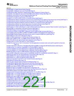
Modified SECCTL register reference place in the note. (Page 142)
Corrected Clock Sequencing table - Removed ALTCORECLK reference, Corrected SYSCLK as CORECLK. (Page 119)
Corrections Applied to I2C Boot Device Configuration Bit Fields (Page 31)
Corrections Applied to Sleep / EMIF16 Boot Device Configuration Bit Fields (Page 29)
Updated Device Configuration Pins Table; PACLKSEL Functional Description (Page 70)
Updated Reset Electrical Data / Timing section. Included updated reset requirements. (Page 130)
Updated Reset Electrical Data; Included updated Reset Requirements. (Page 130)
Updated Table 2-3 Boot Mode Pins: Boot Device Values description of the Ethernet (SGMII) boots. (Page 28)
Removed the SRIOSMGIICLK, MCMCLK, and PCIECLK transition timing values with respect to VOH and VOL within the Main PLL Controller
timing requirements. (Page 142)
Updated Terminal Descriptions of TSIP Pins (Page 51)
Updated EMIF16 timing requirements table (Page 208)
Added MAINPLLCTL1, Renamed DDR3PLLCTL0 to DDR3PLLCT, Renamed PAPLLCTL0 to PAPLLCTL (Page 71)
Corrected the size of TETBs for the 4 cores from 16k to 4k (Page 21)
Corrected the size of TETBs for the 4 cores from 16k to 4k (Page 21)
Updated the complete Power-up sequencing section. RESETFULL must always de-assert after POR (Page 114)
Added section NMI and LRSET. (Page 176)
Corrected Extended Temperature range - Changed 105C to 100C for the top end. (Page 13)
Added BWADJ bit field to DDR3 PLL Control Register. (Page 145)
Added BWADJ bit field to PASS PLL Control Register. (Page 148)
Added MAINPLLCTL1 register table and description. (Page 141)
Added Note on level interrupts and use of EOI handshaking. (Page 157)
Added more detailed information on valid levels for CLKs and IOs during the power sequencing. (Page 114)
Corrected Address Range of I2C MMRs (Page 193)
Corrected PACLKSEL bitfield description. (Page 75)
Corrected RSV01 should be pulled up to 1.8V and RSV08 should be tied to GND (Page 52)
Changed CVDD Range; Corrected CVDD and CVDD1 Descriptions (CVDD: Core Supply -> SR Core Supply) (CVDD1: SR Core Supply -> Core
Supply) (Page 110)
Added more detailed information on valid levels for CLKs and IOs during the power sequencing. (Page 114)
Added to table "Terminal Functions - Signals and Control by Function", signals - RSV0A and RSV0B. (Page 41)
Corrected the timing pointers to point the correct figure (Page 130)
Changed incorrect reserved address in Memory Map Summary - 02780400 -> 02778400 (Page 21)
Corrected Commercial Temperature range - Changed 100C to 85C for the top end. (Page 13)
222
Revision History
Copyright 2012 Texas Instruments Incorporated

 TI [ TEXAS INSTRUMENTS ]