TMS320C6672
Multicore Fixed and Floating-Point Digital Signal Processor
SPRS708C—February 2012
www.ti.com
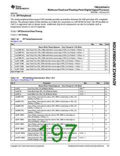
7.13 SPI Peripheral
The serial peripheral interconnect (SPI) module provides an interface between the DSP and other SPI-compliant
devices. The primary intent of this interface is to allow for connection to a SPI ROM for boot. The SPI module on
C6672 is supported only in Master mode. Additional chip-level components can also be included, such as
temperature sensors or an I/O expander.
7.13.1 SPI Electrical Data/Timing
7.13.1.1 SPI Timing
Table 7-66
SPI Timing Requirements
See Figure 7-38)
No.
Min
Max
Unit
Master Mode Timing Diagrams — Base Timings for 3 Pin Mode
7
7
7
7
8
8
8
8
tsu(SOMI-SPC) Input Setup Time, SPIx_SOMI valid before receive edge of SPIx_CLk. Polarity = 0 Phase = 0
tsu(SOMI-SPC) Input Setup Time, SPIx_SOMI valid before receive edge of SPIx_CLk. Polarity = 0 Phase = 1
tsu(SOMI-SPC) Input Setup Time, SPIx_SOMI valid before receive edge of SPIx_CLk. Polarity = 1 Phase = 0
tsu(SOMI-SPC) Input Setup Time, SPIx_SOMI valid before receive edge of SPIx_CLk. Polarity = 1 Phase = 1
th(SPC-SOMI) Input Hold Time, SPIx_SOMI valid after receive edge of SPIx_CLK. Polarity = 0 Phase = 0
th(SPC-SOMI) Input Hold Time, SPIx_SOMI valid after receive edge of SPIx_CLK. Polarity = 0 Phase = 1
th(SPC-SOMI) Input Hold Time, SPIx_SOMI valid after receive edge of SPIx_CLK. Polarity = 1 Phase = 0
th(SPC-SOMI) Input Hold Time, SPIx_SOMI valid after receive edge of SPIx_CLK. Polarity = 1 Phase = 1
2
2
2
2
5
5
5
5
ns
ns
ns
ns
ns
ns
ns
ns
End of Table 7-66
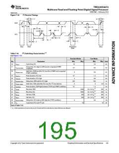
Table 7-67
SPI Switching Characteristics (Part 1 of 2)
(See Figure 7-38 and Figure 7-39)
No.
Parameter
Min
Max
Unit
Master Mode Timing Diagrams — Base Timings for 3 Pin Mode
1
2
3
4
tc(SPC)
Cycle Time, SPIx_CLK, All Master Modes
3*P2 (1)
ns
tw(SPCH)
tw(SPCL)
td(SIMO-SPC)
Pulse Width High, SPIx_CLK, All Master Modes
Pulse Width Low, SPIx_CLK, All Master Modes
0.5*tc - 1
0.5*tc - 1
ns
ns
ns
Setup (Delay), initial data bit valid on SPIx_SIMO to initial edge on SPIx_CLK.
Polarity = 0, Phase = 0.
5
5
5
5
2
2
2
2
4
4
4
5
5
5
5
6
6
td(SIMO-SPC)
td(SIMO-SPC)
td(SIMO-SPC)
td(SPC-SIMO)
td(SPC-SIMO)
td(SPC-SIMO)
td(SPC-SIMO)
toh(SPC-SIMO)
toh(SPC-SIMO)
Setup (Delay), initial data bit valid on SPIx_SIMO to initial edge on SPIx_CLK.
Polarity = 0, Phase = 1.
ns
ns
ns
ns
ns
ns
ns
ns
ns
Setup (Delay), initial data bit valid on SPIx_SIMO to initial edge on SPIx_CLK
Polarity = 1, Phase = 0
Setup (Delay), initial data bit valid on SPIx_SIMO to initial edge on SPIx_CLK
Polarity = 1, Phase = 1
Setup (Delay), subsequent data bits valid on SPIx_SIMO to initial edge on
SPIx_CLK. Polarity = 0 Phase = 0
Setup (Delay), subsequent data bits valid on SPIx_SIMO to initial edge on
SPIx_CLK Polarity = 0 Phase = 1
Setup (Delay), subsequent data bits valid on SPIx_SIMO to initial edge on
SPIx_CLK Polarity = 1 Phase = 0
Setup (Delay), subsequent data bits valid on SPIx_SIMO to initial edge on
SPIx_CLK Polarity = 1 Phase = 1
Output hold time, SPIx_SIMO valid after receive edge of SPIx_CLK except for
final bit. Polarity = 0 Phase = 0
0.5*tc - 2
0.5*tc - 2
Output hold time, SPIx_SIMO valid after receive edge of SPIx_CLK except for
final bit. Polarity = 0 Phase = 1
Copyright 2012 Texas Instruments Incorporated
Peripheral Information and Electrical Specifications 197

 TI [ TEXAS INSTRUMENTS ]