TMS320C6672
Multicore Fixed and Floating-Point Digital Signal Processor
SPRS708C—February 2012
www.ti.com
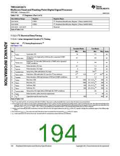
Table 7-63
I2C Registers (Part 2 of 2)
Hex Address Range
0253 0034
Register
ICPID1
ICPID2
-
Register Name
I2C Peripheral Identification Register 1 [Value: 0x0000 0105]
I2C Peripheral Identification Register 2 [Value: 0x0000 0005]
Reserved
0253 0038
0253 003C - 0253 007F
End of Table 7-63
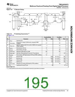
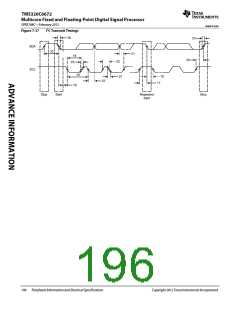
7.12.3 I2C Electrical Data/Timing
7.12.3.1 Inter-Integrated Circuits (I2C) Timing
Table 7-64
I2C Timing Requirements (1)
(see Figure 7-36)
Standard Mode
Fast Mode
No.
Min
Max
Min
Max Units
1
2
tc(SCL)
tsu(SCLH-SDAL)
th(SDAL-SCLL)
Cycle time, SCL
10
2.5
μs
Setup time, SCL high before SDA low (for a repeated START
condition)
4.7
4
0.6
0.6
μs
μs
3
Hold time, SCL low after SDA low (for a START and a repeated
START condition)
4
tw(SCLL)
Pulse duration, SCL low
4.7
4
1.3
0.6
100 (2)
0 (3)
μs
μs
ns
5
tw(SCLH)
tsu(SDAV-SCLH)
th(SCLL-SDAV)
tw(SDAH)
tr(SDA)
Pulse duration, SCL high
6
Setup time, SDA valid before SCL high
Hold time, SDA valid after SCL low (For I2C bus devices)
Pulse duration, SDA high between STOP and START conditions
Rise time, SDA
250
0 (3)
4.7
7
3.45
0.9 (4)
μs
μs
ns
ns
ns
ns
μs
ns
pF
8
1.3
(5)
9
1000 20 + 0.1Cb
1000 20 + 0.1Cb
300 20 + 0.1Cb
300 20 + 0.1Cb
300
300
300
300
(5)
(5)
(5)
10
11
12
13
14
15
tr(SCL)
Rise time, SCL
tf(SDA)
Fall time, SDA
tf(SCL)
Fall time, SCL
tsu(SCLH-SDAH)
tw(SP)
Setup time, SCL high before SDA high (for STOP condition)
Pulse duration, spike (must be suppressed)
Capacitive load for each bus line
4
0.6
0
50
(5)
Cb
400
400
End of Table 7-64
1 The I2C pins SDA and SCL do not feature fail-safe I/O buffers. These pins could potentially draw current when the device is powered down
2 A Fast-mode I2C-bus™ device can be used in a Standard-mode I2C-bus™ system, but the requirement tsu(SDA-SCLH) ≥ 250 ns must then be met. This will automatically be the
case if the device does not stretch the LOW period of the SCL signal. If such a device does stretch the LOW period of the SCL signal, it must output the next data bit to the
SDA line tr max + tsu(SDA-SCLH) = 1000 + 250 = 1250 ns (according to the Standard-mode I2C-Bus Specification) before the SCL line is released.
3 A device must internally provide a hold time of at least 300 ns for the SDA signal (referred to the VIHmin of the SCL signal) to bridge the undefined region of the falling edge
of SCL.
4 The maximum th(SDA-SCLL) has only to be met if the device does not stretch the low period [tw(SCLL)] of the SCL signal.
5 Cb = total capacitance of one bus line in pF. If mixed with HS-mode devices, faster fall-times are allowed.
194
Peripheral Information and Electrical Specifications
Copyright 2012 Texas Instruments Incorporated

 TI [ TEXAS INSTRUMENTS ]