TMS320C6672
Multicore Fixed and Floating-Point Digital Signal Processor
SPRS708C—February 2012
www.ti.com
7.11 DDR3 Memory Controller
The 64-bit DDR3 Memory Controller bus of the TMS320C6672 is used to interface to JEDEC standard-compliant
DDR3 SDRAM devices. The DDR3 external bus interfaces only to DDR3 SDRAM devices; it does not share the bus
with any other types of peripherals.
7.11.1 DDR3 Memory Controller Device-Specific Information
The TMS320C6672 includes one 64-bit wide 1.5-V DDR3 SDRAM EMIF interface. The DDR3 interface can operate
at 800 Mega Transfers per Second (MTS), 1033 MTS, 1333 MTS, and 1600 MTS.
Due to the complicated nature of the interface, a limited number of topologies will be supported to provide a 16-bit,
32-bit, or 64-bit interface.
The DDR3 electrical requirements are fully specified in the DDR Jedec Specification JESD79-3C. Standard DDR3
SDRAMs are available in 8- and 16-bit versions, allowing for the following bank topologies to be supported by the
interface:
•
•
•
•
•
•
•
•
•
•
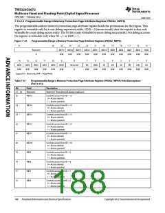
72-bit: Five 16-bit SDRAMs (including 8 bits of ECC)
72-bit: Nine 8-bit SDRAMs (including 8 bits of ECC)
36-bit: Three 16-bit SDRAMs (including 4 bits of ECC)
36-bit: Five 8-bit SDRAMs (including 4 bits of ECC)
64-bit: Four 16-bit SDRAMs
64-bit: Eight 8-bit SDRAMs
32-bit: Two 16-bit SDRAMs
32-bit: Four 8-bit SDRAMs
16-bit: One 16-bit SDRAM
16-bit: Two 8-bit SDRAM
The approach to specifying interface timing for the DDR3 memory bus is different than on other interfaces such as
I2C or SPI. For these other interfaces, the device timing was specified in terms of data manual specifications and I/O
buffer information specification (IBIS) models. For the DDR3 memory bus, the approach is to specify compatible
DDR3 devices and provide the printed circuit board (PCB) solution and guidelines directly to the user.
A race condition may exist when certain masters write data to the DDR3 memory controller. For example, if
master A passes a software message via a buffer in external memory and does not wait for an indication that the write
completes, before signaling to master B that the message is ready, when master B attempts to read the software
message, then the master B read may bypass the master A write and, thus, master B may read stale data and,
therefore, receive an incorrect message.
Some master peripherals (e.g., EDMA3 transfer controllers with TCCMOD=0) will always wait for the write to
complete before signaling an interrupt to the system, thus avoiding this race condition. For masters that do not have
a hardware specification of write-read ordering, it may be necessary to specify data ordering via software.
If master A does not wait for indication that a write is complete, it must perform the following workaround:
1. Perform the required write to DDR3 memory space.
2. Perform a dummy write to the DDR3 memory controller module ID and revision register.
3. Perform a dummy read to the DDR3 memory controller module ID and revision register.
4. Indicate to master B that the data is ready to be read after completion of the read in step 3. The completion of
the read in step 3 ensures that the previous write was done.
Copyright 2012 Texas Instruments Incorporated
Peripheral Information and Electrical Specifications 191

 TI [ TEXAS INSTRUMENTS ]