TMDS361
SLLS919–DECEMBER 2008............................................................................................................................................................................................ www.ti.com
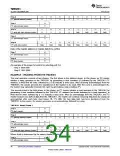
Step 2
7
6
5
4
3
2
1
0
I2C general address (master)
0
1
0
1
1
0
0
0
Step 3
8
I2C acknowledge (slave)
A
Step 4
7
6
5
4
3
2
1
0
I2C write sink logic address (master)
0
0
0
0
Addr
Addr
Addr
Addr
Step 5
8
I2C acknowledge (slave)
A
Step 6
7
6
5
4
3
2
1
0
I2C write data (master)
Data
Data
Data
Data
Data
Data
Data
Data
Data is the register address or register data to be written
Step 7
8
I2C acknowledge (slave)
A
Step 8
0
I2C stop (master)
P
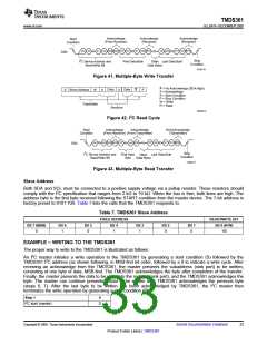
An example of the proper bit control for selecting port 2 is:
Step 4: 0000 0001
Step 6: 1001 0000
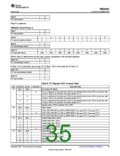
EXAMPLE – READING FROM THE TMDS361
The read operation consists of two phases. The first phase is the address phase. In this phase, an I2C master
initiates a write operation to the TMDS361 by generating a start condition (S) followed by the TMDS361 I2C
address, in MSB-first bit order, followed by a 0 to indicate a write cycle. After receiving acknowledges from the
TMDS361, the master presents the subaddress of the register to be read. After the cycle is acknowledged (A),
the master may optionally terminate the cycle by generating a stop condition (P).
The second phase is the data phase. In this phase, an I2C master initiates a read operation to the TMDS361 by
generating a start condition followed by the TMDS361 I2C address (as shown following for a read operation), in
MSB first bit order, followed by a 1 to indicate a read cycle. After an acknowledge from the TMDS361, the I2C
master receives one byte of data from the TMDS361. The master can continue receiving data byes by issuing an
acknowledge after each byte read (steps 10, 11). After the last data byte has been transferred from the
TMDS361 to the master, the master generates a not-acknowledge followed by a stop.
TMDS361 Read Phase 1
Step 1
0
I2C start (master)
S
Step 2
7
6
5
4
3
2
1
0
I2C general address (master)
0
1
0
1
1
0
0
0
Step 3
8
I2C acknowledge (slave)
A
Step 4
7
6
5
4
3
2
1
0
I2C write sink logic address (master)
0
0
0
0
Addr
Addr
Addr
Addr
Where Addr is determined by the values shown in Table 7.
Step 5
8
I2C acknowledge (slave)
A
34
Submit Documentation Feedback
Copyright © 2008, Texas Instruments Incorporated
Product Folder Link(s) :TMDS361

 TI [ TEXAS INSTRUMENTS ]