TMDS361
www.ti.com ............................................................................................................................................................................................ SLLS919–DECEMBER 2008
Acknowledge
(From Receiver)
Acknowledge
(Receiver)
Acknowledge
(Receiver)
Start
Condition
ACK
ACK
D1 D0
ACK
A6
A5
A1 A0 R/W
D7 D6
D1 D0
D7 D6
SDA
I2C Device Address and
Read/Write Bit
Stop
Condition
Other
Data Bytes
First Data Byte
Last Data Byte
T0397-01
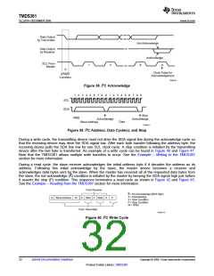
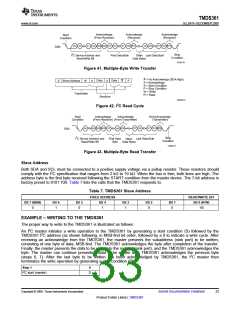
Figure 41. Multiple-Byte Write Transfer
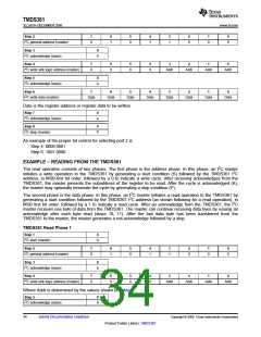
A = No Acknowledge (SDA High)
A = Acknowledge
S = Start Condition
P = Stop Condition
W = Write
W
A
Data
A
Data
A
P
S
Slave Address
Transmitter
R = Read
Receiver
R0008-01
Figure 42. I2C Read Cycle
Start
Condition
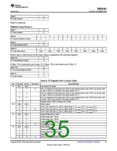
Acknowledge Acknowledge
(From Receiver) (From Transmitter)
Not Acknowledge
(Transmitter)
ACK
ACK
A6
A0
R/W
D7
D0
D7 D6
D1 D0 ACK
SDA
I2C Device Address and
Read/Write Bit
Stop
Condition
First Data
Byte
Other Last Data Byte
Data Bytes
T0398-01
Figure 43. Multiple-Byte Read Transfer
Slave Address
Both SDA and SCL must be connected to a positive supply voltage via a pullup resistor. These resistors should
comply with the I2C specification that ranges from 2 kΩ to 19 kΩ. When the bus is free, both lines are high. The
address byte is the first byte received following the START condition from the master device. The 7-bit address is
factory preset to 0101 100. Table 7 lists the calls that the TMDS361 responds to.
Table 7. TMDS361 Slave Address
FIXED ADDRESS
READ/WRITE BIT
Bit 0 (R/W)
1/0
Bit 7 (MSB)
Bit 6
Bit 5
Bit 4
Bit 3
Bit 2
Bit 1
0
1
0
1
1
0
0
EXAMPLE – WRITING TO THE TMDS361
The proper way to write to the TMDS361 is illustrated as follows:
An I2C master initiates a write operation to the TMDS361 by generating a start condition (S) followed by the
TMDS361 I2C address (as shown following, in MSB-first bit order, followed by a 0 to indicate a write cycle. After
receiving an acknowledge from the TMDS361, the master presents the subaddress (sink port) to be written,
consisting of one byte of data, MSB-first. The TMDS361 acknowledges the byte after completion of the transfer.
Finally, the master presents the data to be written to the register (sink port), and the TMDS361 acknowledges the
byte. The master can continue presenting data to be written after TMDS361 acknowledges the previous byte
(steps 6, 7). After the last byte to be written has been acknowledged by TMDS361, the I2C master then
terminates the write operation by generating a stop condition (P).
Step 1
0
I2C start (master)
S
Copyright © 2008, Texas Instruments Incorporated
Submit Documentation Feedback
33
Product Folder Link(s) :TMDS361

 TI [ TEXAS INSTRUMENTS ]