TMDS361
SLLS919–DECEMBER 2008............................................................................................................................................................................................ www.ti.com
Register 0x01 is read/write.
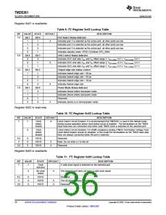
Table 9. I2C Register 0x02 Lookup Table
BIT
VALUE STATE
DEFAULT
DESCRIPTION
7:6
Bit 7
Bit 6
Port Select Status Indicator
1
1
X
Indicates port 1 is selected as the active port, all other ports are low.
Indicates port 2 is selected as the active port, all other ports are low.
Indicates port 3 is selected as the active port, all other ports are low.
Indicates standby mode: HPD[1:3] follows HPD_SINK.
OVS Control Status Indicator
1
0
0
0
0
1
5:4
3:2
Bit 4
Bit 3
0
0
Indicates DDC sink side VOL and VIL offset range 2: VIL2 (max): 0.4 V, VOL2 (max): 0.6 V
Indicates DDC sink side VOL and VIL offset range 3: VIL3 (max): 0.3 V, VOL3 (max): 0.5 V
Indicates DDC sink side VOL and VIL offset range 1: VIL1 (max): 0.4 V, VOL1 (max): 0.7 V
Output edge rate status control
0
1
X
1
1
Bit 3
Bit 2
1
1
Indicates fastest edge rate + 90 ps
1
0
Indicates fastest edge rate + 60 ps
0
1
Indicates fastest edge rate + 30 ps
0
Bit 1
1
0
Bit 0
0
X
X
Indicates fastest edge rate
1:0
Power Mode Status Indicator
Indicates device enters low-power mode
1
1
Indicates device enters low-power mode
0
1
Reserved
0
0
Indicates device is in normal-power mode
Register 0x02 is read-only.
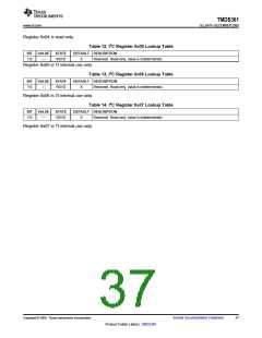
Table 10. I2C Register 0x03 Lookup Table
BIT
VALUE
STATE
DEFAULT
DESCRIPTION
7
1
Clock
detect
enable
X
Clock Detect Circuit Enabled. It is recommended that TMDS361 is used in this default mode
during normal operation where clock detect circuit is enabled . The terminations on the TMDS
input data lines are connected only when valid TMDS clock is detected on the selected port.
0
Clock
detect
disable
Clock Detect Circuit Disabled. For HDMI compliance testing (TMDS Termination Voltage Test)
clock-detect feature should be disabled. In this mode the terminations on the TMDS input data
lines are always connected when the port is selected.
6:5
4
X
0
0
RSVD
RSVD
RSVD
Reserved
X
X
Note: Do not write a 1 to this bit
Reserved
3:0
Register 0x03 is read/write
Table 11. I2C Register 0x04 Lookup Table
BIT
VALUE
STATE
DEFAULT
DESCRIPTION
7
1
Clock
A valid clock signal is detected on the selected port.
detected
0
No clock
detect
X
The selected port does not have a valid clock signal.
6:5
4
X
0
0
RSVD
RSVD
RSVD
Reserved
X
X
This bit should always read 0
Reserved
3:0
36
Submit Documentation Feedback
Copyright © 2008, Texas Instruments Incorporated
Product Folder Link(s) :TMDS361

 TI [ TEXAS INSTRUMENTS ]