TMDS261
www.ti.com ............................................................................................................................................................................................ SLLS953–DECEMBER 2008
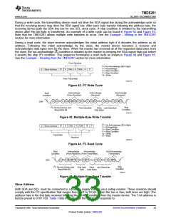
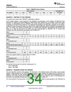
During a write cycle, the transmitting device must not drive the SDA signal line during the acknowledge cycle so
that the receiving device may drive the SDA signal low. After each byte transfer following the address byte, the
receiving device pulls the SDA line low for one SCL clock cycle. A stop condition is initiated by the transmitting
device after the last byte is transferred. An example of a write cycle can be found in Figure 42 and Figure 43.
Note that the TMDS261 allows multiple write transfers to occur. See the Example – Writing to the TMDS261
section for more information.
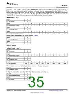
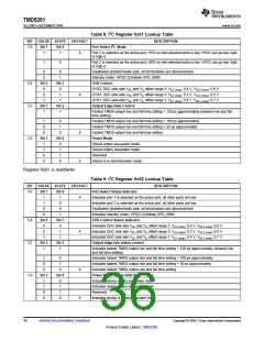
During a read cycle, the slave receiver acknowledges the initial address byte if it decodes the address as its
address. Following this initial acknowledge by the slave, the master device becomes a receiver and
acknowledges data bytes sent by the slave. When the master has received all of the requested data bytes from
the slave, the not-acknowledge (A) condition is initiated by the master by keeping the SDA signal high just before
it asserts the stop (P) condition. This sequence terminates a read cycle as shown in Figure 44 and Figure 45.
See the Example – Reading from the TMDS261 section for more information.
From Receiver
A = No Acknowledge (SDA High)
A = Acknowledge
S = Start Condition
P = Stop Condition
W = Write
W
A
Data
A
Data
A
P
S
Slave Address
From Transmitter
R0007-01
Figure 42. I2C Write Cycle
Acknowledge
(From Receiver)
Acknowledge
(Receiver)
Acknowledge
(Receiver)
Start
Condition
ACK
ACK
D1 D0
ACK
A6
A5
A1 A0 R/W
D7 D6
D1 D0
D7 D6
SDA
I2C Device Address and
Read/Write Bit
Stop
Condition
Other
Data Bytes
First Data Byte
Last Data Byte
T0397-01
Figure 43. Multiple-Byte Write Transfer
A = No Acknowledge (SDA High)
A = Acknowledge
S = Start Condition
P = Stop Condition
W = Write
W
A
Data
A
Data
A
P
S
Slave Address
Transmitter
R = Read
Receiver
R0008-01
Figure 44. I2C Read Cycle
Start
Condition
Acknowledge Acknowledge
(From Receiver) (From Transmitter)
Not Acknowledge
(Transmitter)
ACK
ACK
A6
A0
R/W
D7
D0
D7 D6
D1 D0 ACK
SDA
I2C Device Address and
Read/Write Bit
Stop
Condition
First Data
Byte
Other Last Data Byte
Data Bytes
T0398-01
Figure 45. Multiple-Byte Read Transfer
Slave Address
Both SDA and SCL must be connected to a positive supply voltage via a pullup resistor. These resistors should
comply with the I2C specification that ranges from 2 kΩ to 19 kΩ. When the bus is free, both lines are high. The
address byte is the first byte received following the START condition from the master device. The 7-bit address is
factory preset to 0101 100. Table 7 lists the calls that the TMDS261 responds to.
Copyright © 2008, Texas Instruments Incorporated
Submit Documentation Feedback
33
Product Folder Link(s) :TMDS261

 TI [ TEXAS INSTRUMENTS ]