TMDS261
www.ti.com ............................................................................................................................................................................................ SLLS953–DECEMBER 2008
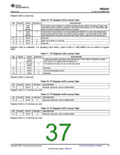
Register 0x02 is read-only.
Table 10. I2C Register 0x03 Lookup Table
BIT
VALUE
STATE
DEFAULT
DESCRIPTION
7
1
Clock
detect
disabled
Clock Detect Circuit Disabled. For HDMI compliance testing (TMDS Termination Voltage Test)
clock-detect feature should be disabled. In this mode the terminations on the TMDS input data
lines are always connected when the port is selected.
0
Clock
detect
enabled
X
Clock Detect Circuit Enabled. It is recommended that TMDS261 is used in this default mode
during normal operation where clock detect circuit is enabled . The terminations on the TMDS
input data lines are connected only when valid TMDS clock is detected on the selected port.
6:5
4
X
0
0
RSVD
RSVD
RSVD
Reserved
X
X
Note: Do not write a 1 to this bit
Reserved
3:0
Register 0x03 is read/write, For disabling clock detect, value of 80h or 1000 0000b can be written to register
0x03.
Table 11. I2C Register 0x04 Lookup Table
BIT
VALUE
STATE
DEFAULT
DESCRIPTION
7
1
Clock
detected
A valid clock signal is detected on the selected port. If clock detect is disabled in register
0x03, then bit 7 of register 0x04 will always be 1.
0
No clock
detect
X
The selected port does not have a valid clock signal.
6:5
4
X
0
0
RSVD
RSVD
RSVD
Reserved
X
X
This bit should always read 0
Reserved
3:0
Register 0x04 is read-only.
Table 12. I2C Register 0x05 Lookup Table
BIT
VALUE
STATE
DEFAULT DESCRIPTION
Reserved. Read-only, value is indeterministic.
7:0
—
RSVD
X
Register 0x05 is TI internal use only.
Table 13. I2C Register 0x06 Lookup Table
BIT
VALUE
STATE
DEFAULT DESCRIPTION
Reserved. Read-only, value is indeterministic.
7:0
—
RSVD
X
Register 0x06 is TI internal use only.
Table 14. I2C Register 0x07 Lookup Table
BIT
VALUE
STATE
DEFAULT DESCRIPTION
7:0
—
RSVD
X
Reserved. Read-only, value is indeterministic.
Register 0x07 is TI internal use only.
Copyright © 2008, Texas Instruments Incorporated
Submit Documentation Feedback
37
Product Folder Link(s) :TMDS261

 TI [ TEXAS INSTRUMENTS ]