TMDS261
SLLS953–DECEMBER 2008............................................................................................................................................................................................ www.ti.com
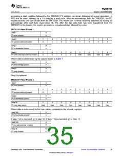
Table 8. I2C Register 0x01 Lookup Table
BIT
VALUE STATE
DEFAULT
DESCRIPTION
7:6
Bit 7
Bit 6
Port Select I2C Mode
1
1
X
Port 1 is selected as the active port; HPD on non-selected ports is low. HPD1 can go low, high
or high-Z.
1
0
Port 2 is selected as the active port; HPD on non-selected ports is low. HPD2 can go low, high
or high-Z.
0
0
Disallowed (indeterminate sate, all terminations are disconnected)
Standby mode: HPD[1:2] follows HPD_SINK.
0
Bit 4
0
1
Bit 3
0
5:4
3:2
OVS Control
OVS2: DDC sink-side VOL and VIL offset range 2: VIL2 (max): 0.4 V, VOL2 (max): 0.6 V
OVS3: DDC sink-side VOL and VIL offset range 3: VIL3 (max): 0.3 V, VOL3 (max): 0.5 V
OVS1: DDC sink-side VOL and VIL offset range 1: VIL1 (max): 0.4 V, VOL1 (max): 0.7 V
Output Edge Rate Control
0
1
X
1
1
Bit 3
1
Bit 2
1
Fastest TMDS output rise and fall time setting + 120 ps approximately (slowest rise and fall
time setting)
1
0
Fastest TMDS output rise and fall time setting + 100 ps approximately
Fastest TMDS output rise and fall time setting + 50 ps approximately
Fastest TMDS output rise and fall time setting
Power Mode
0
1
0
Bit 1
1
0
Bit 0
0
X
X
1:0
Device enters low-power mode.
1
1
Device enters low-power mode.
0
1
Reserved
0
0
Device is in normal-power mode.
Register 0x01 is read/write.
Table 9. I2C Register 0x02 Lookup Table
BIT
VALUE STATE
DEFAULT
DESCRIPTION
Port Select Status Indicator
7:6
Bit 7
Bit 6
1
1
X
Indicates port 1 is selected as the active port, all other ports are low.
Indicates port 2 is selected as the active port, all other ports are low.
Disallowed (indeterminate sate, all terminations are disconnected)
Indicates standby mode: HPD[1:2] follows HPD_SINK.
1
0
0
0
0
Bit 4
0
1
Bit 3
0
5:4
3:2
OVS Control Status Indicator
Indicates DDC sink side VOL and VIL offset range 2: VIL2 (max): 0.4 V, VOL2 (max): 0.6 V
Indicates DDC sink side VOL and VIL offset range 3: VIL3 (max): 0.3 V, VOL3 (max): 0.5 V
Indicates DDC sink side VOL and VIL offset range 1: VIL1 (max): 0.4 V, VOL1 (max): 0.7 V
Output edge rate status control
0
1
X
1
1
Bit 3
1
Bit 2
1
Indicates fastest TMDS output rise and fall time setting + 120 ps approximately (slowest rise
and fall time setting)
1
0
Indicates fastest TMDS output rise and fall time setting + 100 ps approximately
Indicates fastest TMDS output rise and fall time setting + 50 ps approximately
Indicates fastest TMDS output rise and fall time setting
Power Mode Status Indicator
0
1
0
Bit 1
1
0
Bit 0
0
X
X
1:0
Indicates device enters low-power mode
1
1
Indicates device enters low-power mode
0
1
Reserved
0
0
Indicates device is in normal-power mode
36
Submit Documentation Feedback
Copyright © 2008, Texas Instruments Incorporated
Product Folder Link(s) :TMDS261

 TI [ TEXAS INSTRUMENTS ]