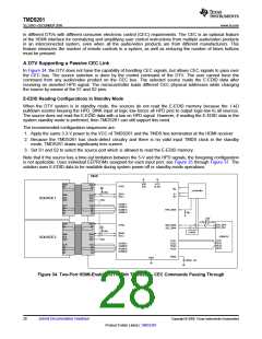
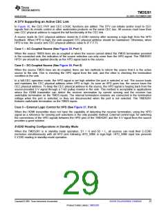
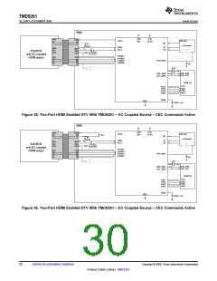
TMDS261
SLLS953–DECEMBER 2008............................................................................................................................................................................................ www.ti.com
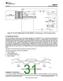
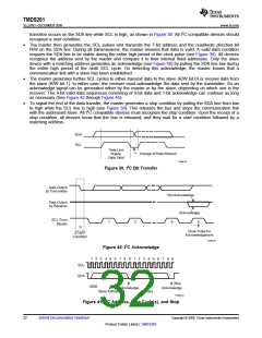
transition occurs on the SDA line while SCL is high, as shown in Figure 38. All I2C-compatible devices should
recognize a start condition.
•
The master then generates the SCL pulses and transmits the 7-bit address and the read/write direction bit
R/W on the SDA line. During all transmissions, the master ensures that data is valid. A valid data condition
requires the SDA line to be stable during the entire high period of the clock pulse (see Figure 39). All devices
recognize the address sent by the master and compare it to their internal fixed addresses. Only the slave
device with a matching address generates an acknowledge (see Figure 40) by pulling the SDA line low during
the entire high period of the ninth SCL cycle. On detecting this acknowledge, the master knows that a
communication link with a slave has been established.
•
•
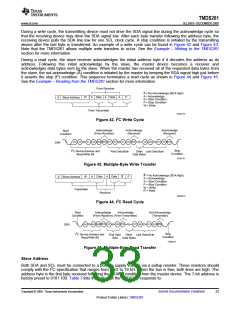
The master generates further SCL cycles to either transmit data to the slave (R/W bit 0) or receive data from
the slave (R/W bit 1). In either case, the receiver must acknowledge the data sent by the transmitter. So an
acknowledge signal can be generated either by the master or by the slave, depending on which one is the
receiver. The 9-bit valid data sequences consisting of 8-bit data and 1-bit acknowledge can continue as long
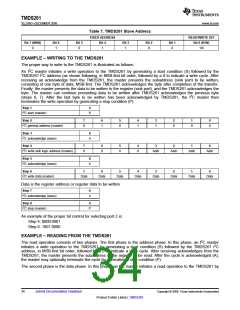
as necessary (See Figure 42 through Figure 45).
To signal the end of the data transfer, the master generates a stop condition by pulling the SDA line from low
to high while the SCL line is high (see Figure 38). This releases the bus and stops the communication link
with the addressed slave. All I2C compatible devices must recognize the stop condition. Upon the receipt of a
stop condition, all devices know that the bus is released, and they wait for a start condition followed by a
matching address.
SDA
SCL
Data Line
Stable;
Data Valid
Change of Data Allowed
T0394-01
Figure 39. I2C Bit Transfer
Data Output
by Transmitter
Not Acknowledge
Data Output
by Receiver
Acknowledge
SCL From
Master
1
2
8
9
S
Clock Pulse for
Acknowledgement
START
Condition
T0395-01
Figure 40. I2C Acknowledge
1
2 3 4 5 6 7 8 9 1 2 3 4 5 6 7 8 9
SCL
SDA
Stop
Acknowledge
MSB
Acknowledge
Slave Address
Data
T0396-01
Figure 41. I2C Address, Data Cycle(s), and Stop
32
Submit Documentation Feedback
Copyright © 2008, Texas Instruments Incorporated
Product Folder Link(s) :TMDS261

 TI [ TEXAS INSTRUMENTS ]