TMDS261
www.ti.com ............................................................................................................................................................................................ SLLS953–DECEMBER 2008
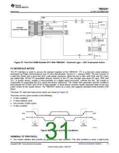
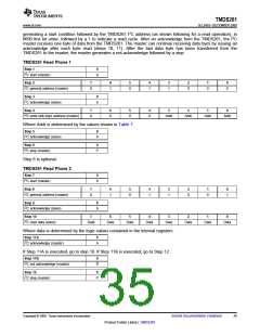
generating a start condition followed by the TMDS261 I2C address (as shown following for a read operation), in
MSB first bit order, followed by a 1 to indicate a read cycle. After an acknowledge from the TMDS261, the I2C
master receives one byte of data from the TMDS261. The master can continue receiving data byes by issuing an
acknowledge after each byte read (steps 10, 11). After the last data byte has been transferred from the
TMDS261 to the master, the master generates a not-acknowledge followed by a stop.
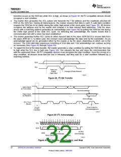
TMDS261 Read Phase 1
Step 1
0
I2C start (master)
S
Step 2
7
6
5
4
3
2
1
0
I2C general address (master)
0
1
0
1
1
0
0
0
Step 3
8
I2C acknowledge (slave)
A
Step 4
7
6
5
4
3
2
1
0
I2C write sink logic address (master)
0
0
0
0
Addr
Addr
Addr
Addr
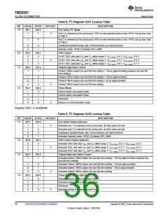
Where Addr is determined by the values shown in Table 7.
Step 5
8
I2C acknowledge (slave)
A
Step 6
0
I2C stop (master)
P
Step 6 is optional.
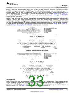
TMDS261 Read Phase 2
Step 7
0
I2C start (master)
S
Step 8
7
6
5
4
3
2
1
0
I2C general address (master)
0
1
0
1
1
0
0
1
Step 9
8
I2C acknowledge (slave)
A
Step 10
7
6
5
4
3
2
1
0
I2C read data (slave)
Data
Data
Data
Data
Data
Data
Data
Data
Where data is determined by the logic values contained in the internal registers.
Step 11A
8
I2C acknowledge (master)
A
If Step 11A is executed, go to step 10. If Step 11B is executed, go to Step 12.
Step 11B
8
I2C not acknowledge (master)
A
Step 12
0
I2C stop (master)
P
Copyright © 2008, Texas Instruments Incorporated
Submit Documentation Feedback
35
Product Folder Link(s) :TMDS261

 TI [ TEXAS INSTRUMENTS ]