TLVM13640
SLVSGJ7 – APRIL 2022
www.ti.com
Limits apply over TJ = –40°C to 125°C, VIN = 24 V, VOUT = 3.3 V, VLDOIN = 5 V, FSW = 800 kHz (unless otherwise noted).
Minimum and maximum limits are specified through production test or by design. Typical values represent the most likely
parametric norm and are provided for reference only.
PARAMETER
TEST CONDITIONS
MIN
TYP
MAX
UNIT
Input current into PG pin when open drain output is
high
IPG
IOV
VPG = 3.3 V
10
nA
Pulldown current at the SW node during an
overvoltage condition
0.5
mA
tPG_FLT_RISE
tPG_FLT_FALL
Delay time to PG high signal
1.5
2.0
2.5
ms
µs
Glitch filter time constant for PG function
120
SWITCHING FREQUENCY
fSW_RANGE Switching frequency range by RT or SYNC
fSW_RT1
200
180
2200
220
kHz
kHz
kHz
Default switching frequency by RRT
Default switching frequency by RRT
RRT = 66.5 kΩ
RRT = 5.76 kΩ
200
fSW_RT2
1980
2200
2420
SYNCHRONIZATION
tB
Blanking of EN after rising or falling edges(1)
4
28
70
µs
V
POWER STAGE
Voltage on CBOOT pin relative to SW that turns off
the high-side switch
VBOOT_UVLO
2.1
VOUT = 1 V, IOUT = 1 A, RBOOT shorted to
CBOOT
tON(min)
tON(max)
tOFF(min)
Minimum ON pulse width(1)
Maximum ON pulse width(1)
Minimum OFF pulse width
55
9
ns
µs
ns
VIN = 4 V, IOUT = 1 A, RBOOT shorted to
CBOOT
65
85
THERMAL SHUTDOWN
TSHD
Thermal shutdown threshold (1)
Thermal shutdown hysteresis (1)
Temperature rising
158
168
10
180
°C
°C
TSHD-HYS
(1) Parameter specified by design, statistical analysis and production testing of correlated parameters. Not production tested.
(2) Production tested with VIN = 3 V.
(3) This is the current used by the device while not switching, open loop, with FB pulled to +5% of nominal. It does not represent the total
input current to the system while regulating.
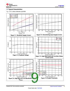
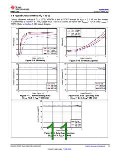
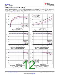
7.6 System Characteristics
The following specifications apply only to the typical applications circuit, with nominal component values. Specifications in the
typical (TYP) column apply to TJ = 25°C only. These specifications are not ensured by production testing.
PARAMETER
TEST CONDITIONS
MIN
TYP
MAX UNIT
SUPPLY
Input supply current when in
regulation
IIN
VIN = VEN = 24 V, VOUT = VVLDOIN = 3.3 V, FSW = 750 kHz, IOUT = 0 A
15
mA
OUTPUT VOLTAGE
ΔVOUT1
ΔVOUT2
ΔVOUT3
Load regulation
VIN = 24 V, VOUT = 3.3 V, IOUT = 0.1 A to 4 A
1
1
mV
mV
mV
Line regulation
Load transient
VOUT = 3.3 V, VIN = 4 V to 36 V, IOUT = 4 A
VIN = 24 V, VOUT = 3.3 V, IOUT = 1 A to 4 A at 1 A/μs, COUT(derated) = 50 μF
100
EFFICIENCY
η
η
η
η
η
Efficiency
VIN = 12 V, VOUT = VVLDOIN = 3.3 V, IOUT = 4 A, FSW = 750 kHz
VIN = 24 V, VOUT = VVLDOIN = 3.3 V, IOUT = 4 A, FSW = 750 kHz
VIN = 12 V, VOUT = VVLDOIN = 5 V, IOUT = 4 A, FSW = 1 MHz
VIN = 24 V, VOUT = VVLDOIN = 5 V, IOUT = 4 A, FSW = 1 MHz
VIN = 24 V, VOUT = VVLDOIN = 12 V, IOUT = 4 A, FSW = 2 MHz
92.1%
91%
Efficiency
Efficiency
Efficiency
Efficiency
94.3%
93%
95.6%
Copyright © 2022 Texas Instruments Incorporated
8
Submit Document Feedback
Product Folder Links: TLVM13640

 TI [ TEXAS INSTRUMENTS ]