TLVM13640
SLVSGJ7 – APRIL 2022
www.ti.com
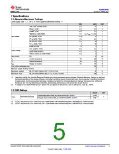
7 Specifications
7.1 Absolute Maximum Ratings
Limits apply over TJ = –40°C to 150°C (unless otherwise noted). (1)
MIN
–0.3
–0.3
–0.3
–0.3
–0.3
–0.3
–0.3
0
MAX
UNIT
V
VIN1, VIN2 to AGND, PGND
RBOOT to SW
42
5.5
V
CBOOT to SW
5.5
V
VLDOIN to AGND, PGND
min (VVIN + 0.3, 16)
V
Input voltage
EN to AGND, PGND
RT to AGND, PGND
FB to AGND, PGND
PG to AGND, PGND
PGND to AGND
42
5.5
16
V
V
V
20
V
–1
2
V
VCC to AGND, PGND
SW to AGND, PGND(2)
VOUT1, VOUT2 to AGND, PGND
PG
–0.3
–0.3
–0.3
5.5
42
V
Output voltage
V
6
V
Input current
10
mA
°C
°C
°C
°C
TJ
Junction temperature
Ambient temperature
Storage temperature
–40
–40
–55
150
125
150
250
3
TA
Tstg
Peak reflow case temperature
Maximum number of reflows allowed
Mechanical vibration
Mechanical shock
MIL-STD-883D, Method 2007.2, 20 Hz to 2 kHz
MIL-STD-883D, Method 2002.3, 1 ms, 1/2 sine, mounted
20
G
G
500
(1) Operation outside the Absolute Maximum Ratings may cause permanent device damage. Absolute Maximum Ratings do not imply
functional operation of the device at these or any other conditions beyond those listed under Recommended Operating Conditions.
If used outside the Recommended Operating Conditions but within the Absolute Maximum Ratings, the device may not be fully
functional, and this may affect device reliability, functionality, performance, and shorten the device lifetime.
(2) A voltage of 2 V below PGND and 2 V above VIN can appear on this pin for ≤ 200 ns with a duty cycle of ≤ 0.01%.
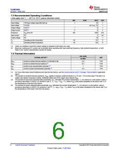
7.2 ESD Ratings
VALUE
±1500
±500
UNIT
Human-body model (HBM), per ANSI/ESDA/JEDEC JS-001(1)
Charged-device model (CDM), per ANSI/ESDA/JEDEC JS-002(2)
V(ESD)
Electrostatic discharge
V
(1) JEDEC document JEP155 states that 500-V HBM allows safe manufacturing with a standard ESD control process.
(2) JEDEC document JEP157 states that 250-V CDM allows safe manufacturing with a standard ESD control process.
Copyright © 2022 Texas Instruments Incorporated
Submit Document Feedback
5
Product Folder Links: TLVM13640

 TI [ TEXAS INSTRUMENTS ]