TLVM13640
SLVSGJ7 – APRIL 2022
www.ti.com
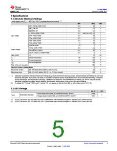
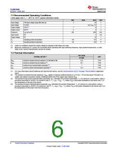
7.3 Recommended Operating Conditions
Limits apply over TJ = –40°C to 125°C (unless otherwise noted).
MIN
NOM
MAX
UNIT
V
Input voltage
Input voltage
Output voltage
Output current
Frequency
Input current
Output voltage
TJ
VIN (input voltage range after start-up)
3
36
VLDOIN
min (VVIN, 12)
V
VOUT(1)
1
0
6
4
V
IOUT(2)
A
FSW set by RT
200
2200
2
kHz
mA
V
PG
PG
16
Operating junction temperature
Operating ambient temperature
–40
–40
125
105
°C
°C
TA
(1) Under no conditions should the output voltage be allowed to fall below zero volts.
(2) Maximum continuous DC current can be derated when operating with high switching frequency, high ambient temperature, or both.
Refer to the Typical Characteristics section for details.
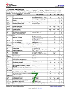
7.4 Thermal Information
RDL (QFN)
THERMAL METRIC(1)
UNIT
20 PINS
22.6
33.1
1
RθJA
RθJA
ψJT
Junction-to-ambient thermal resistance (TLVM13660 EVM)
Junction-to-ambient thermal resistance (2)
°C/W
°C/W
°C/W
°C/W
Junction-to-top characterization parameter (3)
Junction-to-board characterization parameter (4)
ψJB
12.3
(1) For more information about traditional and new thermal metrics, see the Semiconductor and IC Package Thermal Metrics application
report.
(2) The junction-to-ambient thermal resistance, RθJA, applies to devices soldered directly to a 75-mm × 75-mm four-layer PCB with 2 oz.
copper and natural convection cooling. Additional airflow and PCB copper area reduces RθJA
.
(3) The junction-to-top board characterization parameter, ψJT, estimates the junction temperature, TJ, of a device in a real system, using a
procedure described in JESD51-2A (section 6 and 7). TJ = ψJT × PDIS + TT; where PDIS is the power dissipated in the device and TT is
the temperature of the top of the device.
(4) The junction-to-board characterization parameter, ψJB, estimates the junction temperature, TJ, of a device in a real system, using a
procedure described in JESD51-2A (sections 6 and 7). TJ = ψJB × PDIS + TB; where PDIS is the power dissipated in the device and TB is
the temperature of the board 1mm from the device.
Copyright © 2022 Texas Instruments Incorporated
6
Submit Document Feedback
Product Folder Links: TLVM13640

 TI [ TEXAS INSTRUMENTS ]