TLVM13640
SLVSGJ7 – APRIL 2022
www.ti.com
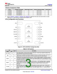
Table 6-1. Pin Functions (continued)
Pin
Type(1)
Description
Name
NO.
Analog ground. Zero-voltage reference for internal references and logic. All electrical parameters are
measured with respect to this pin. These pins must be connected to PGND. See Section 11.2 for a
recommended layout.
AGND
6, 11
G
Internal LDO output. Used as a supply to the internal control circuits. Do not connect to any external
loads. A 1-μF capacitor internally connects from VCC to AGND.
VCC
7
O
P
VOUT1,
VOUT2
Output voltage. These pins are connected to the internal buck inductor. Connect these pins to the output
load and connect external output capacitors between these pins and PGND.
8, 9
Feedback input. Connect the midpoint of the feedback resistor divider to this pin. Connect the upper
resistor (RFBT) of the feedback divider to VOUT at the desired point of regulation. Connect the lower
resistor (RFBB) of the feedback divider to AGND. Do not leave open or connect to ground.
FB
RT
PG
10
12
13
I
I
Frequency setting pin used to set the switching frequency between 200 kHz and 2.2 MHz by placing an
external resistor from RT to AGND. Do not leave open or connect to ground.
Open-drain power-good monitor output that asserts low if the FB voltage is not within the specified
window thresholds. A 10-kΩ to 100-kΩ pullup resistor to a suitable voltage is required. If not used, PG
can be left open or connected to GND.
O
Precision enable input pin. High = on, Low = off. Can be connected to VIN. Precision enable allows
the pin to be used as an adjustable input voltage UVLO. The module can be turned off by using an
open-drain/collector device to connect this pin to AGND. Connect an external resistor divider between
this pin, VIN and AGND to create an external UVLO.
EN
14
15
I
NC
—
G
No connection. Tie to GND or leave open.
Power ground. This is the return current path for the power stage of the device. Connect these pads to
the input supply return, the load return, and the capacitors associated with the VIN and VOUT pins. See
Section 11.2 for a recommended layout.
17, 18,
19, 20
PGND
(1) P = Power, G = Ground, I = Input, O = Output
Copyright © 2022 Texas Instruments Incorporated
4
Submit Document Feedback
Product Folder Links: TLVM13640

 TI [ TEXAS INSTRUMENTS ]