TLVM13640
SLVSGJ7 – APRIL 2022
www.ti.com
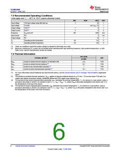
7.5 Electrical Characteristics
Limits apply over TJ = –40°C to 125°C, VIN = 24 V, VOUT = 3.3 V, VLDOIN = 5 V, FSW = 800 kHz (unless otherwise noted).
Minimum and maximum limits are specified through production test or by design. Typical values represent the most likely
parametric norm and are provided for reference only.
PARAMETER
TEST CONDITIONS
MIN
TYP
MAX
UNIT
SUPPLY VOLTAGE
Needed to start up (over the IOUT range)
Once operating (over the IOUT range)
3.95
3
36
36
V
V
VIN
Input operating voltage range
VIN_HYS
IQ_VIN
Hysteresis(1)
1
7
1
V
Input operating quiescent current (non-switching)
VIN shutdown quiescent current
TA = 25°C, VEN = 3.3 V, VFB = 1.5 V
VEN = 0 V, TA = 25°C
µA
µA
ISDN_VIN
ENABLE
VEN_RISE
VEN_FALL
VEN_HYS
VEN_WAKE
IEN
EN voltage rising threshold
EN voltage falling threshold
EN voltage hysteresis
1.161
1.263
0.91
1.365
0.404
V
V
0.303
0.4
0.353
V
EN wake-up threshold
V
Input current into EN (non-switching)
EN high to start of switching delay(1)
VEN = 3.3 V, VFB = 1.5 V
10
nA
ms
tEN
0.7
VCC INTERNAL LDO
3.4 V ≤ VVLDOIN ≤ 12.5 V
VVLDOIN = 3.1 V, non-switching
VVLDOIN < 3.1 V(1)
3.3
3.1
3.6
3.6
1.1
25
V
V
VCC
Internal LDO VCC voltage
V
VCC_UVLO
VCC UVLO rising threshold
VIN < 3.6 V(2)
V
VCC_UVLO_HYS VCC UVLO hysteresis(2)
Hysteresis below VCC_UVLO
VEN = 3.3 V, VFB = 1.5 V
V
IVLDOIN
FEEDBACK
VOUT
Input current into VLDOIN pin (non-switching)(3)
31
6
µA
Adjustable output voltage range
Feedback voltage
Over the IOUT range
TA = 25°C, IOUT = 0 A
1
V
V
VFB
1.0
Over the VIN range, VOUT = 1 V, IOUT = 0
A, FSW = 200 kHz
VFB_ACC
Feedback voltage accuracy
–1%
+1%
VFB
Load regulation
Line regulation
TA = 25°C, 0 A ≤ IOUT ≤ 6 A
TA = 25°C, IOUT = 0 A, 4 V ≤ VIN ≤ 36 V
VFB = 1 V
0.1%
0.1%
10
VFB
IFB
Input current into FB
nA
CURRENT
IOUT
Output current
TA = 25°C
0
4
A
A
A
A
A
IOCL
Output overcurrent (DC) limit threshold
High-side switch current limit
Low-side switch current limit
Negative current limit
5.9
7.0
4.8
–3
IL_HS
IL_LS
IL_NEG
Duty cycle approaches 0%
6.0
4.0
8.1
5.4
Ratio of FB voltage to in-regulation FB voltage to
enter hiccup
VHICCUP
tW
Not during soft start
40%
80
Short circuit wait time ("hiccup" time before soft start)
ms
(1)
SOFT START
tSS
Time from first SW pulse to VFB at 90%
VIN ≥ 4.2 V
VIN ≥ 4.2 V
3.5
9.5
5
7
ms
ms
Time from first SW pulse to release of FPWM lockout
if output not in regulation(1)
tSS2
13
17
POWER GOOD
PGOV
PG upper threshold – rising
% of VOUT setting
105%
92%
107%
94%
110%
PGUV
PG lower threshold – falling
% of VOUT setting
96.5%
PGHYS
PG threshold hysteresis (rising and falling)
Input voltage for valid PG output
PG low-level output voltage
% of VOUT setting
1.3%
VIN_PG_VALID
VPG_LOW
46-μA pullup, VEN = 0 V
2-mA pullup to PG pin, VEN = 3.3 V
1.0
V
V
0.4
Copyright © 2022 Texas Instruments Incorporated
Submit Document Feedback
7
Product Folder Links: TLVM13640

 TI [ TEXAS INSTRUMENTS ]