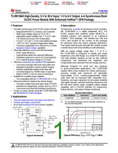
TLVM13640
SLVSGJ7 – APRIL 2022
www.ti.com
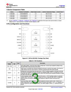
5 Device Comparison Table
Device
Orderable Part Number
Rated Output Current
Junction Temperature Range
–40°C to 125°C
External Sync(1)
TLVM13620
TLVM13630
TLVM13640
TLVM13660
TLVM13620RDHR
TLVM13630RDHR
TLVM13640RDLR
TLVM13660RDLR
2 A
3 A
4 A
6 A
No
No
No
No
–40°C to 125°C
–40°C to 125°C
–40°C to 125°C
(1) See the TPSM63602, TPSM63603, TPSM63604, and TPSM63606 for applications that require clock synchronization, an output
voltage above 6 V, spread-spectrum modulation for EMI mitigation or both.
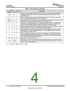
6 Pin Configuration and Functions
1
16
VIN1
VIN2
17
PGND
SW
CBOOT
RBOOT
VLDOIN
AGND
2
3
4
5
6
7
15
14
13
12
11
10
NC
EN
18
PGND
PG
RT
19
AGND
FB
PGND
VCC
20
PGND
8
9
VOUT1
VOUT2
Figure 6-1. 20-Pin QFN RDL Package (Top View)
Table 6-1. Pin Functions
Pin
Type(1)
Description
Name
NO.
Input supply voltage. Connect the input supply to these pins. Connect input capacitors between these
pins and PGND in close proximity to the device.
VIN1, VIN2
SW
1, 16
P
Switch node. Do not place any external component on this pin or connect to any signal. The amount of
copper placed on this pin must be kept to a minimum to prevent issues with noise and EMI.
2
3
O
Bootstrap pin for the internal high-side gate driver. A 100-nF bootstrap capacitor is internally connected
from this pin to SW within the module to provide the bootstrap voltage. CBOOT is brought out to use in
conjunction with RBOOT to effectively lower the value of the internal series bootstrap resistance to adjust
the switch-node slew rate, if necessary.
CBOOT
RBOOT
VLDOIN
I/O
I/O
P
External bootstrap resistor connection. Internal to the device, a 100-Ω bootstrap resistor is connected
between RBOOT and CBOOT. RBOOT is brought out to use in conjunction with CBOOT to effectively
lower the value of the internal series bootstrap resistance to adjust the switch-node slew rate, if
necessary.
4
5
Input bias voltage. Input to the internal LDO that supplies the internal control circuits. Connect to an
output voltage point to improve efficiency. Connect an optional high-quality 0.1-μF to 1-μF capacitor from
this pin to ground for improved noise immunity. If the output voltage is above 12 V, connect this pin to
ground.
Copyright © 2022 Texas Instruments Incorporated
Submit Document Feedback
3
Product Folder Links: TLVM13640

 TI [ TEXAS INSTRUMENTS ]