TLVM13640
SLVSGJ7 – APRIL 2022
www.ti.com
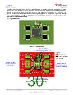
11 Layout
Proper PCB design and layout is important in high-current, fast-switching module circuits (with high internal
voltage and current slew rates) to achieve reliable device operation and design robustness. Furthermore, the
EMI performance of the module depends to a large extent on PCB layout.
11.1 Layout Guidelines
The following list summarizes the essential guidelines for PCB layout and component placement to optimze
DC/DC module performance, including thermals and EMI signature. Figure 11-1 and Figure 11-2 show a
recommended PCB layout for the TLVM13640 with optimized placement and routing of the power-stage and
small-signal components.
•
Place input capacitors as close as possible to the VIN pins. Note the dual and symmetrical arrangement
of the input capacitors based on the VIN1 and VIN2 pins located on each side of the module package.
The high-frequency currents are split in two and effectively flow in opposing directions such that the related
magnetic fields contributions cancel each other, leading to improved EMI performance.
– Use low-ESR 1206 or 1210 ceramic capacitors with X7R or X7S dielectric. The module has integrated
dual 0402 input capacitors for high-frequency bypass.
– Ground return paths for the input capacitors should consist of localized top-side planes that connect to the
PGND pads under the module.
– Even though the VIN pins are connected internally, use a wide polygon plane on a lower PCB layer to
connect these pins together and to the input supply.
•
•
Place output capacitors as close as possible to the VOUT pins. A similar dual and symmetrical arrangement
of the output capacitors enables magnetic field cancellation and EMI mitigation.
– Ground return paths for the output capacitors should consist of localized top-side planes that connect to
the PGND pads under the module.
– Even though the VOUT pins are connected internally, use a wide polygon plane on a lower PCB layer to
connect these pins together and to the load, thus reducing conduction loss and thermal stress.
Keep the FB trace as short as possible by placing the feedback resistors close to the FB pin. Reduce noise
sensitivity of the output voltage feedback path by placing the resistor divider close to the FB pin, rather than
close to the load. FB is the input to the voltage-loop error anplifier and represents a high-impedance node
sensitive to noise. Route a trace from the upper feedback resistor to the required point of output voltage
regulation.
•
•
Use a solid ground plane on the PCB layer directly below the top layer with the module. This plane acts as
a noise shield by minimizing the magnetic fields associated with the currents in the switching loops. Connect
AGND pins 6 and 11 directly to PGND pin 19 under the module.
Provide enough PCB area for proper heatsinking. Use sufficient copper area to acheive a low thermal
impedance commensurate with the maximum load current and ambient temperature conditions. Provide
adequate heatsinking for the TLVM13640 to keep the junction temperature below 150°C. For operation at
full rated load, the top-side ground plane is an important heat-dissipating area. Use an array of heat-sinking
vias to connect the exposed pads (PGND) of the package to the PCB ground plane. If the PCB has multiple
copper layers, connect these thermal vias to inner-layer ground planes. Make the top and bottom PCB layers
preferably with two-ounce copper thickness (and no less than one ounce).
11.1.1 Thermal Design and Layout
For a DC/DC module to be useful over a particular temperature range, the package must allow for the efficient
removal of the heat produced while keeping the junction temperature within rated limits. The TLVM13640 module
is available in a small 5.5-mm × 5-mm 20-pin QFN (RDL) package to cover a range of application requirements.
The Thermal Information table summarizes the thermal metrics of this package with related detail provided by
the Semiconductor and IC Package Thermal Metrics Application Report.
The 20-pin QFN package offers a means of removing heat through the exposed thermal pads at the base of
the package. This allows a significant improvement in heatsinking, and it becomes imperative that the PCB
is designed with thermal lands, thermal vias, and one or more ground planes to complete the heat removal
subsystem. The exposed pads of the TLVM13640 are soldered to the ground-connected copper lands on the
PCB directly underneath the device package, reducing the thermal resistance to a very low value.
Copyright © 2022 Texas Instruments Incorporated
Submit Document Feedback
29
Product Folder Links: TLVM13640

 TI [ TEXAS INSTRUMENTS ]