TLVM13640
SLVSGJ7 – APRIL 2022
www.ti.com
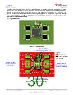
Preferably, use a four-layer board with 2-oz copper thickness for all layers to provide low impedance, proper
shielding and lower thermal resistance. Numerous vias with a 0.3-mm diameter connected from the thermal
lands to the internal and solder-side ground planes are vital to promote heat transfer. In a multi-layer PCB
stack-up, a solid ground plane is typically placed on the PCB layer below the power-stage components. Not only
does this provide a plane for the power-stage currents to flow, but it also represents a thermally conductive path
away from the heat-generating device.
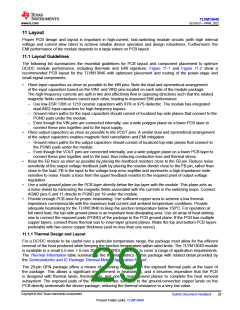
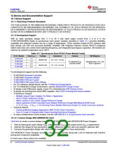
11.2 Layout Example
Figure 11-1. Typical Layout
Place the feedback
components close to the FB pin
Legend
Top layer copper
EN
Layer-2 GND plane
RT
VIN
VIN
VOUT
Input
capacitor
Top solder
Output
capacitor
FB
Position the input
capacitors very close
to the VIN pins
Place an array of
PGND vias close to the
IC for heat spreading
PGND
Input
capacitor
Output
capacitor
VOUT
Place thermal vias at the
VOUT pins for heat spreading
Figure 11-2. Typical Top Layer Design
Copyright © 2022 Texas Instruments Incorporated
30
Submit Document Feedback
Product Folder Links: TLVM13640

 TI [ TEXAS INSTRUMENTS ]