TLVM13640
SLVSGJ7 – APRIL 2022
www.ti.com
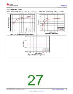
9.2.2.3 Application Curves
Unless otherwise indicated, VIN = 24 V, VOUT = –5 V, IOUT = –3 A (1.66-Ω resistive load), and FSW = 1.2 MHz.
100
95
90
85
80
75
70
VIN = 12 V
VIN = 24 V
65
0
0.5
1
1.5
2
2.5
3
3.5
Output Current (A)
Figure 9-12. Efficiency
Figure 9-11. IBB Maximum Output Current
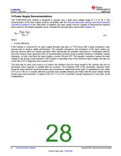
-5.05
-5.025
-5
-4.975
-4.95
VIN = 12 V
VIN = 24 V
0
0.5
1
1.5
2
2.5
3
3.5
Output Current (A)
Figure 9-13. Load Regulation
Copyright © 2022 Texas Instruments Incorporated
Submit Document Feedback
27
Product Folder Links: TLVM13640

 TI [ TEXAS INSTRUMENTS ]