TLVM13640
SLVSGJ7 – APRIL 2022
www.ti.com
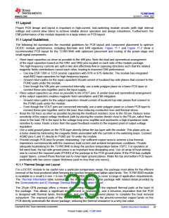
9.2.2 Design 2 – Inverting Buck-Boost Regulator with Negative Output Voltage
Figure 9-10 shows the schematic diagram of an inverting buck-boost (IBB) regulator with an output of –5 V at –3
A and a switching frequency of 1.2 MHz. In this example, the target half-load and full-load efficiencies are 90%
and 90.5%, respectively, based on a nominal input voltage of 24 V that ranges from 10 V to 31 V.
VIN+
U1
CIN3
10
VIN1
VIN2
VIN = 10 V to 31 V
VIN–
VIN(on) = 8.9 V
F
CIN1
10
CIN2
10
F
F
PGND
PGND
RENT
604 k
–VOUT
–VOUT
Optional
TLVM13640
Precision
EN
VLDOIN
external bias
enable for
VIN UVLO
VOUT+
VOUT1
VOUT2
CBOOT
VCC
RENB
100 k
VOUT = –5 V
IOUT(max) = –3 A
COUT
PG
RT
RFBT
3 ꢀ 47
F
RBOOT
FB
102 k
–VOUT
VOUT–
–VOUT
RRT
10.7 k
RFBB
AGND
25.5 k
–VOUT
Figure 9-10. Circuit Schematic
9.2.2.1 Design Requirements
Table 9-3 shows the intended input, output, and performance parameters for this application example. With an
IBB topology, the module sees a total current of IIN + |–IOUT|, which is highest at minimum input voltage.
Table 9-3. Design Parameters
Design Parameter
Input voltage range
Input voltage UVLO turn on
Output voltage
Value
10 V to 31 V
8.9 V
–5 V
Full-load current
–3 A
Switching frequency
Output voltage regulation
1.2 MHz
±1%
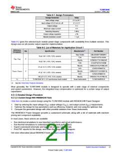
Table 9-4 gives the selected buck module power-stage components with availability from multiple vendors. This
design uses an all-ceramic output capacitor implementation.
Table 9-4. List of Materials for Application Circuit 2
Ref Des
Qty
Specification
Manufacturer(1)
Part Number
Kemet
C1210C106K5RACTU
CNA6P1X7R1H106K
GRM32ER71A476ME15L
GRT32EC70J107ME13L
TLVM13640RDLR
CIN1, CIN2, CIN3
3
10 µF, 50 V, X7R, 1210, ceramic
TDK
47 µF, 10 V, X7R, 1210, ceramic
Murata
COUT1, COUT2
U1
2
1
100 µF, 6.3 V, X7S, 1210, ceramic
Murata
TLVM13640 36-V, 4-A synchronous buck module
Texas Instruments
(1) See the Third-Party Products Disclaimer.
Copyright © 2022 Texas Instruments Incorporated
Submit Document Feedback
25
Product Folder Links: TLVM13640

 TI [ TEXAS INSTRUMENTS ]