TCA6424A
www.ti.com
SCPS193B –JULY 2010–REVISED SEPTEMBER 2010
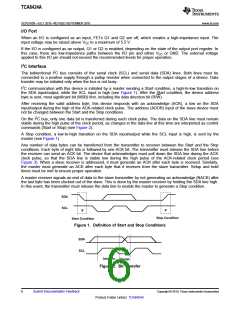
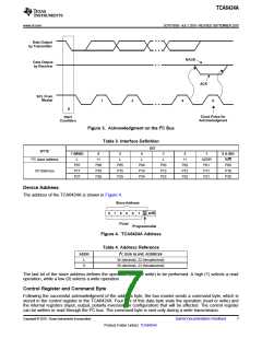
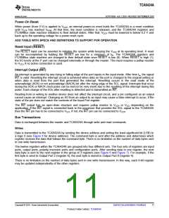
Data Output
by Transmitter
NACK
Data Output
by Receiver
ACK
SCL From
Master
1
2
8
9
S
Clock Pulse for
Acknowledgment
Start
Condition
Figure 3. Acknowledgment on the I2C Bus
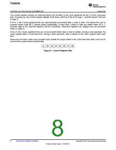
Table 3. Interface Definition
BIT
BYTE
7 (MSB)
6
5
4
3
2
1
0 (LSB)
I2C slave address
L
H
L
L
L
H
ADDR
P01
R/W
P00
P10
P20
P07
P17
P27
P06
P16
P26
P05
P15
P25
P04
P14
P24
P03
P13
P23
P02
P12
P22
I/O data bus
P11
P21
Device Address
The address of the TCA6424A is shown in Figure 4.
Slave Address
AD
0
1
0
1
R/W
DR
0
0
Fixed
Programmable
Figure 4. TCA6424A Address
Table 4. Address Reference
ADDR
I2C BUS SLAVE ADDRESS
34 (decimal), 22 (hexadecimal)
35 (decimal), 23 (hexadecimal)
L
H
The last bit of the slave address defines the operation (read or write) to be performed. A high (1) selects a read
operation, while a low (0) selects a write operation.
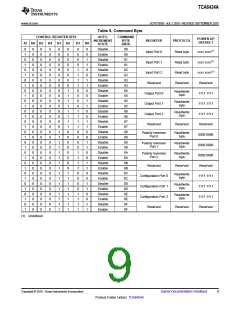
Control Register and Command Byte
Following the successful acknowledgment of the address byte, the bus master sends a command byte, which is
stored in the control register in the TCA6424A. Four bits of this data byte state the operation (read or write) and
the internal registers (input, output, polarity inversion, or configuration) that will be affected. The control register
can be written or read through the I2C bus. The command byte is sent only during a write transmission.
Copyright © 2010, Texas Instruments Incorporated
Submit Documentation Feedback
7
Product Folder Link(s): TCA6424A

 TI [ TEXAS INSTRUMENTS ]