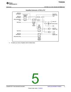
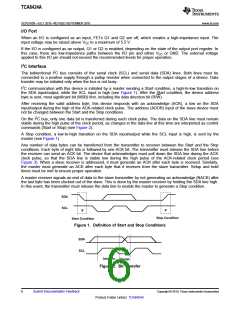
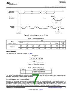
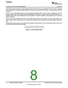
PDF
最近搜索
热门搜索
发布采购

| 型号: | TCA6424A |
| PDF下载: | 下载PDF文件 查看货源 |
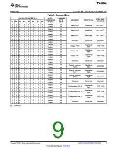
| 内容描述: | 低压24位I2C和SMBus I / O扩展器,带有中断输出,复位和配置寄存器 [LOW-VOLTAGE 24-BIT I2C AND SMBus I/O EXPANDER WITH INTERRUPT OUTPUT RESET AND CONFIGURATION REGISTERS] |
| 分类和应用: | 输出元件 |
| 文件页数/大小: | 33 页 / 540 K |
| 品牌: |  TI [ TEXAS INSTRUMENTS ] TI [ TEXAS INSTRUMENTS ] |
专业IC领域供求交易平台:提供全面的IC Datasheet资料和资讯,Datasheet 1000万数据,IC品牌1000多家。