TCA6424A
SCPS193B –JULY 2010–REVISED SEPTEMBER 2010
www.ti.com
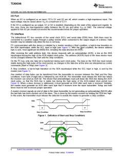
Register Descriptions
The Input Port registers (registers 0, 1 and 2) reflect the incoming logic levels of the pins, regardless of whether
the pin is defined as an input or an output by the Configuration register. They act only on read operation. Writes
to these registers have no effect. The default value (X) is determined by the externally applied logic level. Before
a read operation, a write transmission is sent with the command byte to indicate to the I2C device that the Input
Port register will be accessed next.
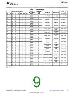
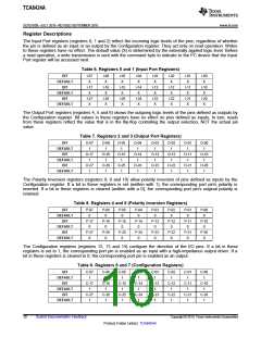
Table 6. Registers 0 and 1 (Input Port Registers)
BIT
DEFAULT
BIT
I-07
X
I-06
X
I-05
X
I-04
X
I-03
X
I-02
X
I-01
X
I-00
X
I-17
X
I-16
X
I-15
X
I-14
X
I-13
X
I-12
X
I-11
X
I-10
X
DEFAULT
BIT
I-27
X
I-26
X
I-25
X
I-24
X
I-23
X
I-22
X
I-21
X
I-20
X
DEFAULT
The Output Port registers (registers 4, 5 and 6) shows the outgoing logic levels of the pins defined as outputs by
the Configuration register. Bit values in these registers have no effect on pins defined as inputs. In turn, reads
from these registers reflect the value that is in the flip-flop controlling the output selection, NOT the actual pin
value.
Table 7. Registers 2 and 3 (Output Port Registers)
BIT
DEFAULT
BIT
O-07
1
O-06
1
O-05
1
O-04
1
O-03
1
O-02
1
O-01
1
O-00
1
O-17
1
O-16
1
O-15
1
O-14
1
O-13
1
O-12
1
O-11
1
O-10
1
DEFAULT
BIT
O-27
1
O-26
1
O-25
1
O-24
1
O-23
1
O-22
1
O-21
1
O-20
1
DEFAULT
The Polarity Inversion registers (registers 8, 9 and 10) allow polarity inversion of pins defined as inputs by the
Configuration register. If a bit in these registers is set (written with 1), the corresponding port pin's polarity is
inverted. If a bit in these registers is cleared (written with a 0), the corresponding port pin's original polarity is
retained.
Table 8. Registers 4 and 5 (Polarity Inversion Registers)
BIT
DEFAULT
BIT
P-07
0
P-06
0
P-05
0
P-04
0
P-03
0
P-02
0
P-01
0
P-00
0
P-17
0
P-16
0
P-15
0
P-14
0
P-13
0
P-12
0
P-11
0
P-10
0
DEFAULT
BIT
P-27
0
P-26
0
P-25
0
P-24
0
P-23
0
P-22
0
P-21
0
P-20
0
DEFAULT
The Configuration registers (registers 12, 13 and 14) configure the direction of the I/O pins. If a bit in these
registers is set to 1, the corresponding port pin is enabled as an input with a high-impedance output driver. If a
bit in these registers is cleared to 0, the corresponding port pin is enabled as an output.
Table 9. Registers 6 and 7 (Configuration Registers)
BIT
DEFAULT
BIT
C-07
1
C-06
1
C-05
1
C-04
1
C-03
1
C-02
1
C-01
1
C-00
1
C-17
1
C-16
1
C-15
1
C-14
1
C-13
1
C-12
1
C-11
1
C-10
1
DEFAULT
BIT
C-27
1
C-26
1
C-25
1
C-24
1
C-23
1
C-22
1
C-21
1
C-20
1
DEFAULT
10
Submit Documentation Feedback
Copyright © 2010, Texas Instruments Incorporated
Product Folder Link(s): TCA6424A

 TI [ TEXAS INSTRUMENTS ]