TCA6424A
www.ti.com
SCPS193B –JULY 2010–REVISED SEPTEMBER 2010
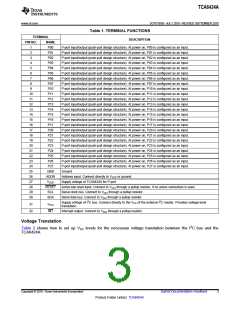
Table 1. TERMINAL FUNCTIONS
TERMINAL
DESCRIPTION
PIN NO.
1
NAME
P00
P01
P02
P03
P04
P05
P06
P07
P10
P11
P12
P13
P14
P15
P16
P17
P20
P21
P22
P23
P24
P25
P26
P27
GND
ADDR
VCCP
RESET
SCL
SDA
P-port input/output (push-pull design structure). At power on, P00 is configured as an input.
P-port input/output (push-pull design structure). At power on, P01 is configured as an input.
P-port input/output (push-pull design structure). At power on, P02 is configured as an input.
P-port input/output (push-pull design structure). At power on, P03 is configured as an input.
P-port input/output (push-pull design structure). At power on, P04 is configured as an input.
P-port input/output (push-pull design structure). At power on, P05 is configured as an input.
P-port input/output (push-pull design structure). At power on, P06 is configured as an input.
P-port input/output (push-pull design structure). At power on, P07 is configured as an input.
P-port input/output (push-pull design structure). At power on, P10 is configured as an input.
P-port input/output (push-pull design structure). At power on, P11 is configured as an input.
P-port input/output (push-pull design structure). At power on, P12 is configured as an input.
P-port input/output (push-pull design structure). At power on, P13 is configured as an input.
P-port input/output (push-pull design structure). At power on, P14 is configured as an input.
P-port input/output (push-pull design structure). At power on, P15 is configured as an input.
P-port input/output (push-pull design structure). At power on, P16 is configured as an input.
P-port input/output (push-pull design structure). At power on, P17 is configured as an input.
P-port input/output (push-pull design structure). At power on, P20 is configured as an input.
P-port input/output (push-pull design structure). At power on, P21 is configured as an input.
P-port input/output (push-pull design structure). At power on, P22 is configured as an input.
P-port input/output (push-pull design structure). At power on, P23 is configured as an input.
P-port input/output (push-pull design structure). At power on, P24 is configured as an input.
P-port input/output (push-pull design structure). At power on, P25 is configured as an input.
P-port input/output (push-pull design structure). At power on, P26 is configured as an input.
P-port input/output (push-pull design structure). At power on, P27 is configured as an input.
Ground
2
3
4
5
6
7
8
9
10
11
12
13
14
15
16
17
18
19
20
21
22
23
24
25
26
27
28
29
30
Address input. Connect directly to VCCP or ground.
Supply voltage of TCA6424A for P port
Active-low reset input. Connect to VCCI through a pullup resistor, if no active connection is used.
Serial clock bus. Connect to VCCI through a pullup resistor.
Serial data bus. Connect to VCCI through a pullup resistor.
Supply voltage of I2C bus. Connect directly to the VCC of the external I2C master. Provides voltage-level
translation.
31
32
VCCI
INT
Interrupt output. Connect to VCCI through a pullup resistor.
Voltage Translation
Table 2 shows how to set up VCC levels for the necessary voltage translation between the I2C bus and the
TCA6424A.
Copyright © 2010, Texas Instruments Incorporated
Submit Documentation Feedback
3
Product Folder Link(s): TCA6424A

 TI [ TEXAS INSTRUMENTS ]