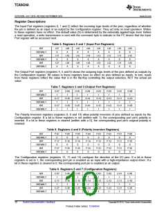
TCA6424A
SCPS193B –JULY 2010–REVISED SEPTEMBER 2010
www.ti.com
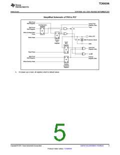
I/O Port
When an I/O is configured as an input, FETs Q1 and Q2 are off, which creates a high-impedance input. The
input voltage may be raised above VCC to a maximum of 5.5 V.
If the I/O is configured as an output, Q1 or Q2 is enabled, depending on the state of the output port register. In
this case, there are low-impedance paths between the I/O pin and either VCC or GND. The external voltage
applied to this I/O pin should not exceed the recommended levels for proper operation.
I2C Interface
The bidirectional I2C bus consists of the serial clock (SCL) and serial data (SDA) lines. Both lines must be
connected to a positive supply through a pullup resistor when connected to the output stages of a device. Data
transfer may be initiated only when the bus is not busy.
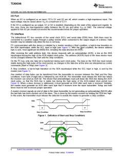
I2C communication with this device is initiated by a master sending a Start condition, a high-to-low transition on
the SDA input/output, while the SCL input is high (see Figure 1). After the Start condition, the device address
byte is sent, most significant bit (MSB) first, including the data direction bit (R/W).
After receiving the valid address byte, this device responds with an acknowledge (ACK), a low on the SDA
input/output during the high of the ACK-related clock pulse. The address (ADDR) input of the slave device must
not be changed between the Start and the Stop conditions.
On the I2C bus, only one data bit is transferred during each clock pulse. The data on the SDA line must remain
stable during the high pulse of the clock period, as changes in the data line at this time are interpreted as control
commands (Start or Stop) (see Figure 2).
A Stop condition, a low-to-high transition on the SDA input/output while the SCL input is high, is sent by the
master (see Figure 1).
Any number of data bytes can be transferred from the transmitter to receiver between the Start and the Stop
conditions. Each byte of eight bits is followed by one ACK bit. The transmitter must release the SDA line before
the receiver can send an ACK bit. The device that acknowledges must pull down the SDA line during the ACK
clock pulse, so that the SDA line is stable low during the high pulse of the ACK-related clock period (see
Figure 3). When a slave receiver is addressed, it must generate an ACK after each byte is received. Similarly,
the master must generate an ACK after each byte that it receives from the slave transmitter. Setup and hold
times must be met to ensure proper operation.
A master receiver signals an end of data to the slave transmitter by not generating an acknowledge (NACK) after
the last byte has been clocked out of the slave. This is done by the master receiver by holding the SDA line high.
In this event, the transmitter must release the data line to enable the master to generate a Stop condition.
SDA
SCL
S
P
Stop Condition
Start Condition
Figure 1. Definition of Start and Stop Conditions
SDA
SCL
Data Line
Change
Figure 2. Bit Transfer
6
Submit Documentation Feedback
Copyright © 2010, Texas Instruments Incorporated
Product Folder Link(s): TCA6424A

 TI [ TEXAS INSTRUMENTS ]