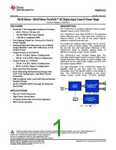
TAS5614LA
www.ti.com
SLAS846 –MAY 2012
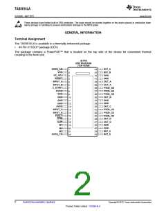
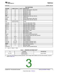
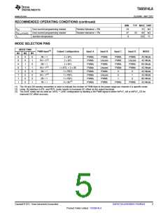
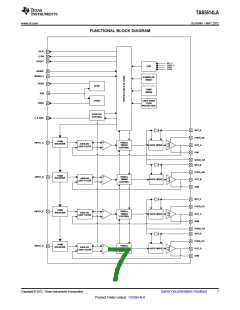
PIN FUNCTIONS
DESCRIPTION
PIN NAME
AVDD
PINOUT DDV-44
I/O/P(1)
13
44
43
24
23
18
7
P
P
P
P
P
O
O
P
O
Internal voltage regulator, analog section
Bootstrap pin, A-side
BST_A
BST_B
BST_C
BST_D
CLIP
Bootstrap pin, B-side
Bootstrap pin, C-side
Bootstrap pin, D-side
Clipping warning; open drain; active low
Startup ramp
C_START
DVDD
8
Internal voltage regulator, digital section
Shutdown signal, open drain; active low
FAULT
16
9, 10, 11, 12, 25,
26, 33, 34, 41, 42
GND
P
Ground
GVDD_AB
GVDD_CD
INPUT_A
INPUT_B
INPUT_C
INPUT_D
M1
1
P
P
I
Gate-drive voltage supply; AB-side
Gate-drive voltage supply; CD-side
PWM Input signal for half-bridge A
PWM Input signal for half-bridge B
PWM Input signal for half-bridge C
PWM Input signal for half-bridge D
Mode selection 1 (LSB)
22
5
6
I
14
I
15
I
19
I
M2
20
I
Mode selection 2
M3
21
I
Mode selection 3 (MSB)
OC_ADJ
OTW
3
O
O
O
O
O
O
P
P
I
Over-Current threshold programming pin
Over-temperature warning; open drain; active low
Output, half-bridge A
17
39, 40
35
OUT_A
OUT_B
OUT_C
OUT_D
PVDD_AB
PVDD_CD
RESET
VDD
Output, half-bridge B
32
Output, half-bridge C
27, 28
36, 37, 38
29, 30, 31
4
Output, half-bridge D
PVDD supply for half-bridge A and B
PVDD supply for half-bridge C and D
Device reset Input; active low
Input power supply
2
P
P
PowerPAD™
Ground, connect to grounded heat sink
(1) I = Input, O = Output, P = Power
Table 1. ORDERING INFORMATION(1)
TA
PACKAGE
DESCRIPTION
TAS5614LADDV
TAS5614LADDVR
0°C–70°C
44 pin HTSSOP
(1) For the most current package and ordering information, see the Package Option Addendum at the end of this document, or see the TI
website at www.ti.com.
Copyright © 2012, Texas Instruments Incorporated
Submit Documentation Feedback
3
Product Folder Link(s): TAS5614LA

 TI [ TEXAS INSTRUMENTS ]